Semiconductor VC Series③: Designing for Volatility
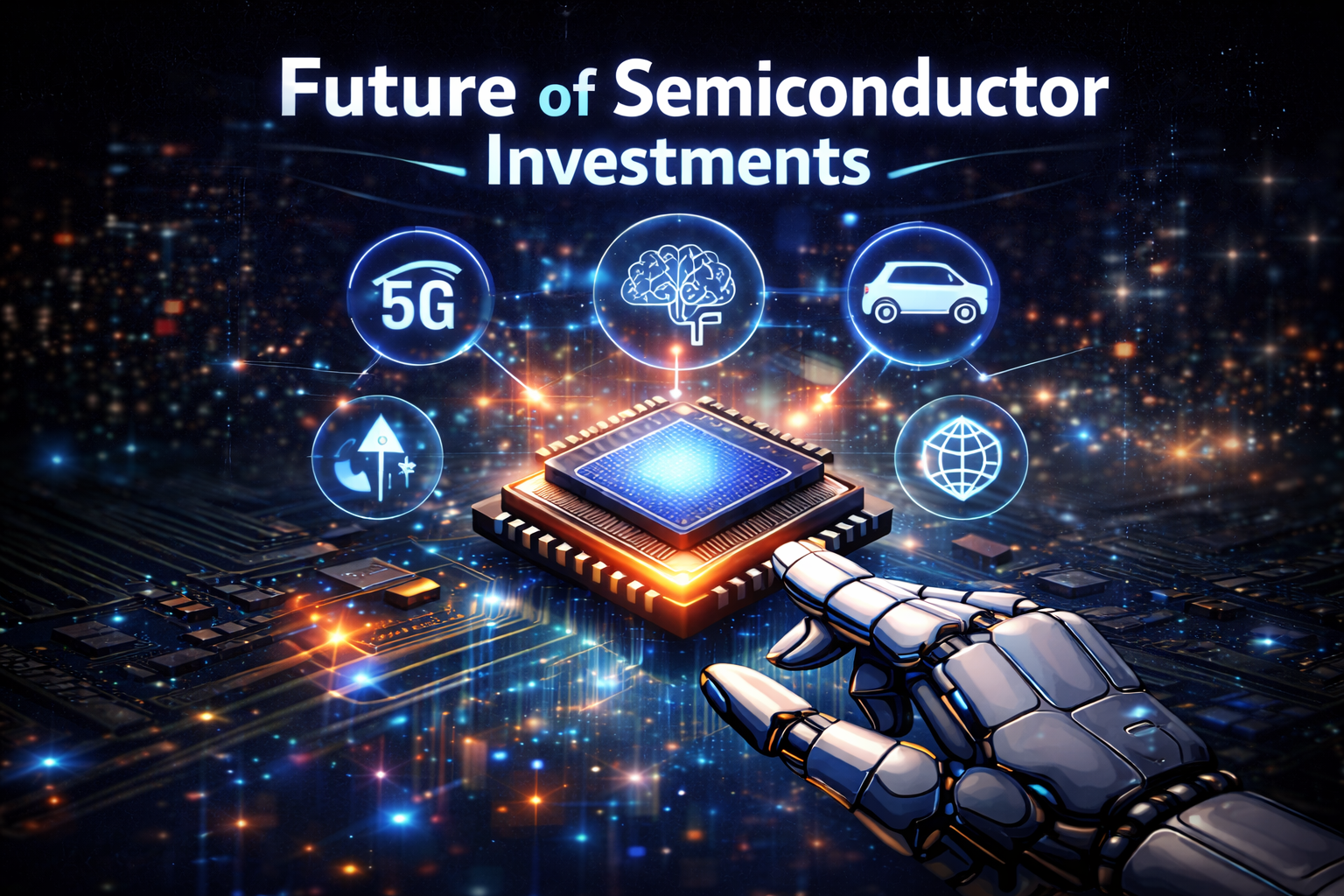
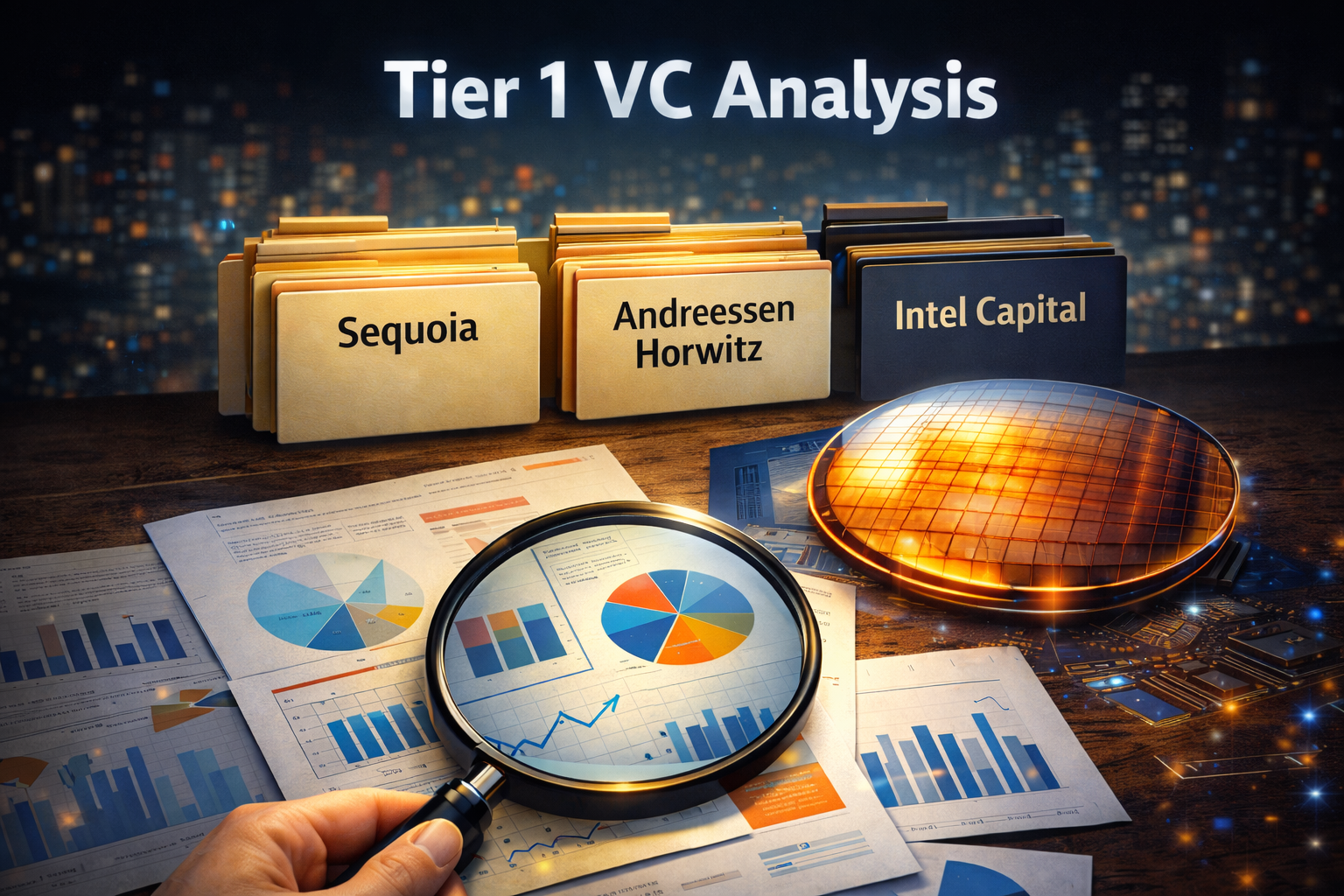
Why Tier-1 VCs decompose semiconductor investing into "design productivity, data movement, packaging, supply chain" rather than betting on chips alone — short, mid, and long-term opportunities and risks systematized from a process-engineering CVC view.
Why Tier-1 VCs decompose semiconductor investing into "design productivity, data movement, packaging, supply chain" rather than betting on chips alone — short, mid, and long-term opportunities and risks systematized from a process-engineering CVC view.


Semiconductor VC: Designing for Volatility
I came up through the floor — leading EEPROM volume production and yield improvement on the process side. Semiconductor cyclicality isn't a textbook abstraction for me; it's something I felt in my bones across more than four product ramps. You can't reliably surf the cycle, but you can take structural positions that are immune to it. That's the conclusion I've arrived at after watching Tier-1 VCs for a decade, and that's the lens that ties this final installment together.
What "Designing for Volatility" Means
Let me reset the question flat first.
The semiconductor industry is inherently cyclical. Demand explodes, supply catches up 2–3 years later, prices collapse — the history of semiconductors has always been one of boom and bust. But when Tier-1 VCs commit hundreds of millions of dollars to semiconductor startups today, they are not trying to "ride the cycle." They are targeting structural positions that are immune to the cycle itself.
This is what "designing for volatility" means: investing in standardized interface technologies (CPO, UCIe) whose demand remains stable even when chip prices swing wildly; design infrastructure (EDA automation, IP reuse) that becomes more valuable with every chip generation transition; and software-defined computing foundations that are independent of any specific hardware vendor — bets on layers where price competition doesn't dominate.
In this final installment, I synthesize the strategy, technology, and deal data from Parts 1 and 2 into four key frameworks:
- Comparative analysis of five Tier1 VCs and the essence of their strategic differences
- Investment opportunities and risks across short (≤18 months), medium (2–4 years), and long (5+ years) time horizons
- Macro environment summary: market size, equipment investment, and policy
- Implications for individual investors, institutional investors, and corporate strategists

Executive Summary
① The "AI demand → semiconductor bottleneck → startup opportunity" structure will persist beyond 2026 As long as GPU performance scaling continues, bottlenecks in design, data movement, and packaging will remain unsolved. Tier1 VCs have already anticipated this structural demand with major investments executed in 2023–2025.
② VC firms' investment "styles" diverge sharply: ecosystem model vs. vertical integration model While Sequoia and a16z build ecosystems through diversified investments in startup clusters, SoftBank concentrates capital in large single-company vertical integration bets (e.g., Ampere at $6.5B valuation). Kleiner Perkins focuses on the U.S. manufacturing revival thesis with clear IPO paths, while Bessemer emphasizes synergies with its existing data center infrastructure portfolio.
③ Long-term, "new computing paradigms" offer the highest non-linear return potential — but commercialization risk is high Analog computing, quantum, and photonics all carry low near-term expected values, but successful commercialization creates non-linear return gaps versus conventional approaches. VCs hold these as "options" within diversified portfolios, using medium-term certainties to stabilize overall returns.
Tier1 VC Strategy Comparison: The Essence of Differences
| VC | Investment Style | Signature Deals | Ecosystem/Partnership Structure | Expected Exit |
|---|---|---|---|---|
| Sequoia Capital | Diversified ecosystem. Early-stage bets across design automation and novel computing paradigms | Ricursive ($35M), Unconventional Computing ($475M) | Network bridges portfolio companies to NVIDIA, Synopsys, Coreweave | M&A (EDA majors) or IPO (compute infra) |
| Andreessen Horowitz (a16z) | Thematic, large concentrated bets on "AI factory" infrastructure spanning data movement and next-gen memory | Ayar Labs ($500M), Nexthop AI ($500M) | Commercial pipeline formation with cloud providers (AWS, Azure, GCP) | M&A by data center operators or IPO |
| Kleiner Perkins | Policy/manufacturing revival theme. CHIPS Act beneficiaries, U.S. onshoring thesis | Retym ($75M), Kandou Technologies ($92.3M) | SEMI association, U.S. DoD/DARPA program linkages | IPO (market enthusiasm for CHIPS Act beneficiaries) |
| Bessemer Venture Partners | Data center infrastructure synergy. Prioritizes fit with existing cloud investment portfolio | Quantum Circuits ($60M+), ChipAgents ($21M) | Customer sharing with existing cloud/SaaS portfolio companies | M&A (cloud majors internalizing capabilities) |
| SoftBank Vision Fund | Vertical integration, mega-rounds. Concentrated capital in single companies; group synergy prioritized | Ampere Computing ($6.5B valuation), Graphcore acquisition | Vertical integration with SB group (Arm, T-Mobile, residual WeWork network) | Long-term hold or IPO (Arm IPO as precedent) |
The Essential Divide: Ecosystem vs. Vertical Integration
Ecosystem Model (Sequoia / a16z / KP / Bessemer)
────────────────────────────────────────────────
VC
 ├── Startup A (Design Automation)
 ├── Startup B (Interconnect/CPO)
 ├── Startup C (Advanced Packaging)
 └── Startup D (New Computing Paradigm)
        │
        ▼
 Portfolio companies form mutual customer-supplier relationships
 → VC itself becomes the hub of a self-reinforcing ecosystem

Vertical Integration Model (SoftBank)
────────────────────────────────────────────────
SoftBank
 └── Ampere Computing (proprietary Arm CPU design)
      └── IP licensed from Arm (SB subsidiary)
           └── Direct-to-data-center sales model
                → Full value chain captured within the group
Investment Opportunities and Risks: Three Time Horizons
Short-Term (≤18 Months): Design Efficiency and EDA Automation
| Opportunity | Investment Theme | Representative Startups | Key Risks |
|---|---|---|---|
| EDA Automation | LLM-powered circuit verification and bug correction reducing design time by 30–50% | Ricursive (Seq.), ChipAgents (Bessemer) | Synopsys/Cadence accelerating in-house LLM development; acquisition risk |
| IP Reuse/Modularization | AI-powered search and customization of existing IP assets reducing new chip design cost | Multiple undisclosed stealth-stage companies | Leading fabs (TSMC, Samsung) building proprietary IP libraries, crowding out differentiation |
| Supply Chain Visibility | Geopolitical risk driving demand for SaaS platforms that map procurement uncertainty | (Numerous undisclosed companies) | In a recession, software spend is the first to be cut |
Short-term investment criteria: Can the company acquire initial customers within 18 months? Is the model software-first and insulated from regulatory risk? EDA automation meets these conditions, but the large R&D budgets of Cadence and Synopsys demand constant vigilance.
Medium-Term (2–4 Years): Data Movement, CPO, and Advanced Packaging
| Opportunity | Investment Theme | Representative Startups | Key Risks |
|---|---|---|---|
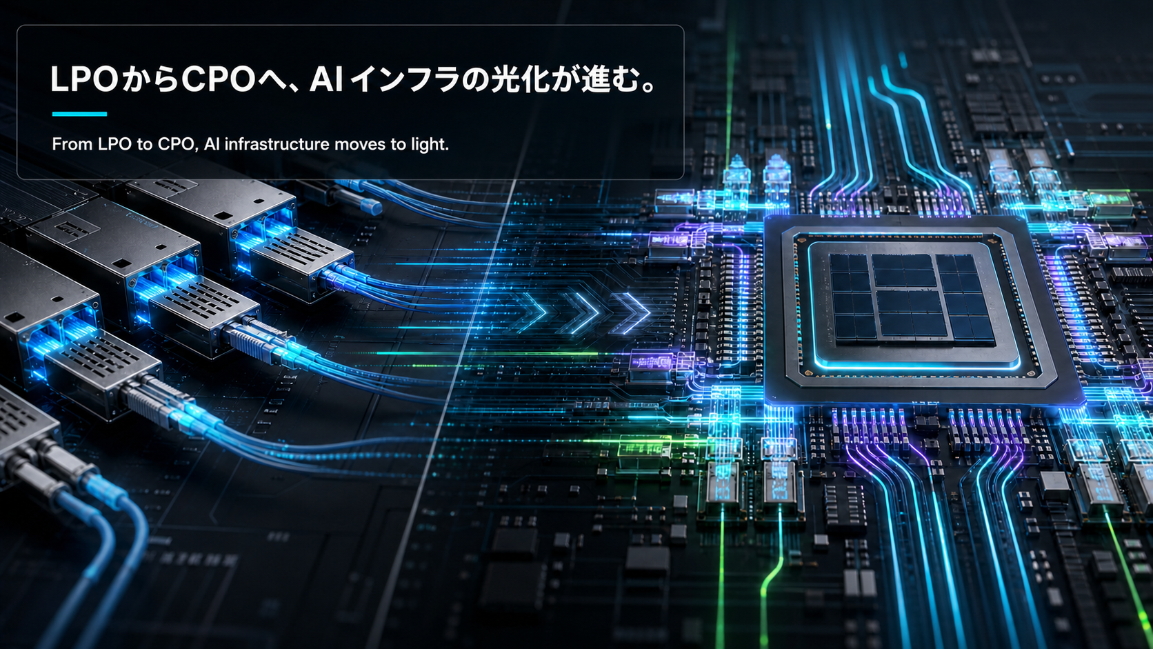
| CPO (Co-Packaged Optics) | Replacing copper GPU-to-memory interconnect with optical fiber; 10× bandwidth, 60–80% power reduction | Ayar Labs (a16z, $500M) | Production yield (optical component manufacturing complexity); TSMC/Intel CPO internalization risk |
| High-Speed SerDes and Electrical Interconnect | Extending copper's lifespan by improving intra-data-center wiring efficiency | Kandou Technologies (KP, $92.3M) | Legacy risk if optical migration happens faster than expected |
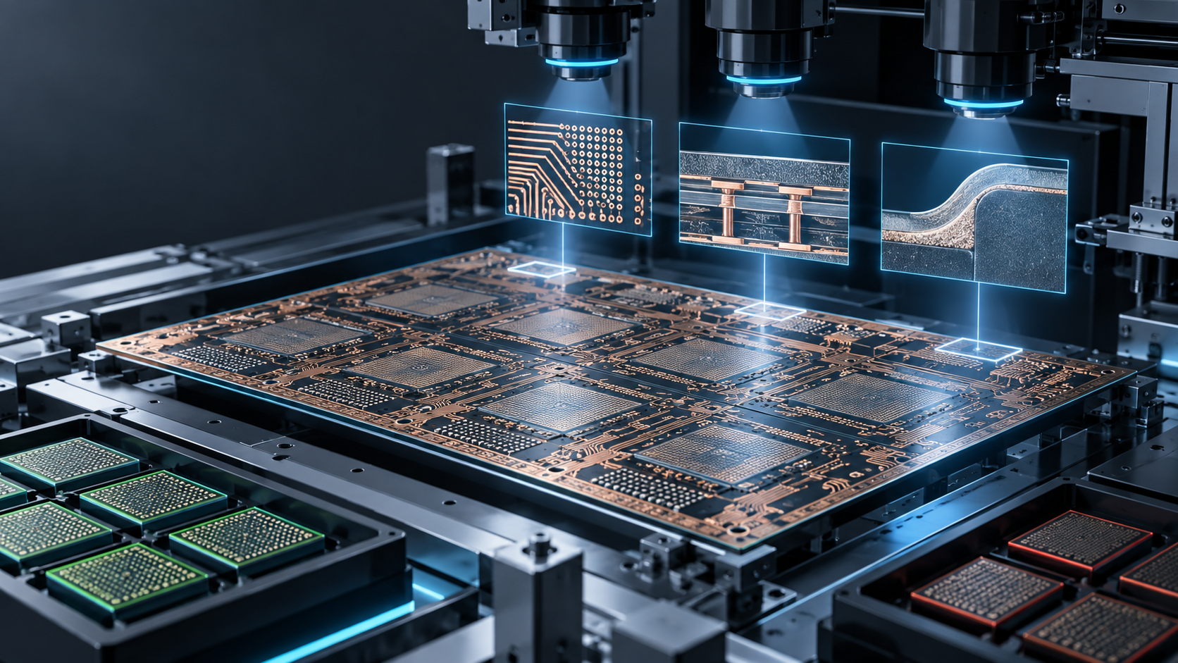
| Advanced Packaging (Chiplet/3D IC) | Heterogeneous chip integration via Chiplet standards (UCIe) | Nexthop AI (a16z, $500M) | IP ownership negotiation complexity between fabless companies and foundries |
| Next-Gen Memory Interfaces | Redesigning bandwidth vs. power tradeoffs as HBM3/4 successors | (Startups co-developing with SK Hynix, Micron) | DRAM vendors' growing in-house development capacity making third parties redundant |
Medium-term investment criteria: Does the company compete with TSMC's, Samsung's, or Intel's advanced packaging expansion plans? If so, has it established a JDA (Joint Development Agreement) partnership? This is a matter of survival. Ayar Labs' co-development structure with TSMC, backed by a16z, is the canonical example.
Long-Term (5+ Years): New Computing Paradigms and Quantum
| Opportunity | Investment Theme | Representative Startups | Key Risks |
|---|---|---|---|
| Analog Computing | Eliminating digital conversion overhead; 100× inference power reduction for edge AI | Unconventional Computing (Seq., $475M) | Programmability (generality) limitations; underdeveloped developer ecosystem |
| Quantum Computing | Exceeding classical computation in prime factorization, quantum chemistry simulation, optimization | Quantum Circuits (Bessemer, $60M+), Rigetti ($79M) | Error correction maturity; identifying commercial use cases that achieve "quantum advantage" |
| Photonic Computing | Using light for matrix operations to dramatically reduce AI inference power consumption | (Multiple undisclosed companies) | Immature silicon photonics manufacturing infrastructure; scale-up cost |
| Neuromorphic Computing | Asynchronous computation mimicking neural circuits; ultra-low-power sensor processing | (Multiple academic spinouts) | Difficult to adapt for general-purpose compute; unclear path from niche markets |
Long-term investment criteria: Is there a clear "paper → product → market" connection? For quantum, the volume of papers and patents is world-class, but companies that cannot show a path to commercial error rates should be approached with caution. Analog computing, by contrast, has a well-defined target market in edge inference, making medium-to-long-term commercialization scenarios more legible.
Macro Environment: Market Size, Equipment Investment, and Policy
| Metric | 2024 Actual | 2025 Forecast | 2026 Forecast | 2027 Forecast | Source |
|---|---|---|---|---|---|
| Global Semiconductor Market | $627B | $791.7B | $975B | $1.1T+ | WSTS Autumn 2025 |
| 300mm Equipment Spending | $107B | $119B | $133B | $151B | SEMI 2026 Forecast |
| AI Semiconductors (GPU/NPU/ASIC) | $130B | $200B+ | $280B+ | $380B+ | IDC/Gartner estimates |
| U.S. CHIPS Act Grants Executed | $8B | $30B+ | $52B (cap) | — | U.S. Commerce Dept. |
| China Semiconductor Export Controls | HBM + EDA | EUV export ban continues | Further tightening expected | — | BIS/METI |
How Policy Environment Affects Investment Decisions
CHIPS Act / EU Chips Act
    │
    ├── Direct beneficiaries (Intel Foundry, TSMC Arizona, Samsung Texas)
    │        └── → Indirect demand for construction/equipment/materials startups
    │
    └── Elevated priority on geopolitical risk management
             └── → Accelerated VC capital flow into U.S.-designed/manufactured startups

China Export Controls (BIS)
    │
    ├── Sales restrictions on AI chips to China (H800 → H20)
    │        └── → China's domestic semiconductor self-sufficiency investment explodes (Huawei/Cambricon)
    │
    └── Advanced EDA/equipment export ban to China
             └── → Reflexive benefit for Western startups (Chinese competitors' capability constrained)
Portfolio Construction Framework
Reading across the actual portfolio allocations of Tier1 VCs reveals a consistent three-layer structure by time horizon:
Ideal Portfolio Allocation by Time Horizon (Illustrative)
──────────────────────────────────────────────────────
Short-term (≤18 months)   ████████████████░░░░  40%
  └── EDA automation · Design SaaS · Supply chain visibility

Medium-term (2–4 years)   ██████████████████░░  45%
  └── CPO · Interconnect · Advanced packaging · AI accelerators

Long-term (5+ years)      ██████░░░░░░░░░░░░░░  15%
  └── Analog computing · Quantum · Photonics · Neuromorphic
──────────────────────────────────────────────────────
Implications for Individual Investors
Individual investors rarely have direct access to VC funds, but indirect semiconductor startup exposure is available through:
- Listed semiconductor companies (NVIDIA, ASML, Lam Research, TSMC ADR): Direct customers of startups, benefitting directly from the bottlenecks that startups are solving
- Semiconductor ETFs (SOXX, SMH): Diversification benefit, but large-cap weighted — limited startup growth reflection
- SPACs and secondary markets: Companies like Rigetti (quantum), which went public via SPAC, offer individual investors high-risk, high-volatility access
- Corporate parents of active CVCs: Investing in SoftBank Group, Intel (Intel Capital parent), or Qualcomm (Qualcomm Ventures parent) provides indirect VC portfolio exposure
Implications for Institutional Investors and Corporates
- LPs (endowments, pension funds): Commitments to Sequoia / a16z / Bessemer align well with long-term semiconductor themes, but require capital that can tolerate the J-Curve (returns typically negative for 3–5 years post-commitment)
- Corporate CVC: Identify the bottleneck in your own value chain and strategically invest in the startup addressing it — simultaneously acquiring M&A optionality and competitive intelligence
Series Wrap-Up and Next Focal Points
What the Three-Part Series Revealed
| Part | Core Message |
|---|---|
| Part 1: Overview and Key Players | Tier1 VCs are concentrating on the "structural absence" at AI infrastructure bottlenecks. The common pattern is decomposing investment across four layers — design, movement, packaging, and supply chain — rather than betting on chips themselves |
| Part 2: Technology Deep Dives | Approximately $2.5B in investment was concentrated across EDA automation, CPO, advanced packaging, and new computing paradigms from 2022–2025. Technical maturity and commercial path clarity determine deal size |
| Part 3: Strategic Implications (this piece) | VC styles bifurcate into ecosystem vs. vertical integration models. Short-term returns come from software profitability; medium-term from CPO/packaging; long-term from analog/quantum |
Focal Points for H2 2026 and Beyond
- Ayar Labs volume production timeline: Will a16z's $500M CPO bet reach volume manufacturing in 2026–2027? Achieving commercial yield rates (90%+) will determine the pace of CPO adoption across the entire industry
- Ampere Computing IPO: If SoftBank's hinted 2026 IPO for Ampere materializes, it will provide the first publicly available data on Arm-based CPU market share in data centers
- CHIPS Act Phase 2 grants: U.S. Commerce Department's second-round grant decisions in H2 2026 (expanding beyond foundries to design, materials, and EDA companies) could accelerate capital flows to startups
- China's advanced fabrication breakthrough: Given Huawei's demonstrated 7nm-equivalent Kirin/Ascend chips, the timing of any sub-5nm breakthrough will determine both Western regulatory response speed and the persistence of the "technology gap"
- Quantum error correction hitting commercial tolerances: Whether Google (Willow), IBM, and Microsoft's logical qubit implementations can connect to commercial use cases (financial optimization, drug discovery) by 2027–2028
ZYL0's Take
The essence of semiconductor investment is infrastructure lock-in. GPUs alone, memory alone — neither creates sustainable differentiation. But the data-movement technology bridging them (CPO, SerDes), the upstream design-efficiency layer (EDA automation), and the downstream assembly layer (advanced packaging) all have the kind of stickiness that resists easy substitution once adopted.
Tier-1 VCs concentrating $2.5B+ in these areas is the rational outcome of a simple observation: they don't want to be dragged into chip price competition. Price wars are manufacturing's destiny, but infrastructure can achieve software-like network effects. From having watched the same dynamic play out in process IP, equipment data, and yield-improvement know-how on the floor, I think this framing is right.
What this series reinforced for me is that semiconductors are inseparable from geopolitics. The CHIPS Act, BIS export controls, Japan's economic security legislation — these policy variables influence investment decisions at least as much as pure technical assessment.
For individual investors engaging with the semiconductor sector: tracking the policy calendar alongside the technology roadmap is no longer optional. It's table stakes.
Next Issue Ideas
- Idea 1: A data-updated follow-up — Revisit the thesis with fresh numbers and separate what strengthened from what broke.
- Idea 2: A practical template edition — Turn the article into a checklist readers can reuse for investing, pricing, or technical operations.
- Idea 3: The bear-case test — Define the conditions that would invalidate this view and map the indicators to watch next.
Related Posts
- Semiconductor VC Series①: Converging on AI Bottlenecks — Where are Tier-1 VCs placing bets in the expanding $975B semiconductor market? Strategies of Sequoia, a16z, Kleiner Pe…
- Why Design, Data Movement & Packaging Attract VC Capital — Series② — As GPU performance scales, design, I/O, and packaging become the real AI bottleneck.
- How to Read Optical I/O Startups From the Outside: Insertion Loss, Thermals, Manufacturability, and Customer Validation — An outside-in checklist for reading optical I/O startups from public information: insertion loss, thermals, manufacturing yield, and customer validation.
References
The factual and numerical assumptions in this article are anchored to primary or public materials that readers can revisit during AdSense review and future updates.
This article is for informational purposes only and does not constitute investment advice or a recommendation of any specific stock, service, or contract structure. The author may hold positions or interests related to companies or services mentioned. Generative AI was used for parts of research, translation, and proofreading, with final review by ZYL0. See the disclaimer for details.