Elephantech Copper Interconnect Technology: Where P-Flex, DeepVia, and DS-SAP Change PCB Manufacturing
A process-level comparison of Elephantech copper nanoparticle technology across surface traces, HDI vias, and package substrates, separating production evidence from evaluations and reproducing a copper-material calculation.
A process-level comparison of Elephantech copper nanoparticle technology across surface traces, HDI vias, and package substrates, separating production evidence from evaluations and reproducing a copper-material calculation.


Elephantech Copper Interconnect Technology: Where P-Flex, DeepVia, and DS-SAP Change PCB Manufacturing
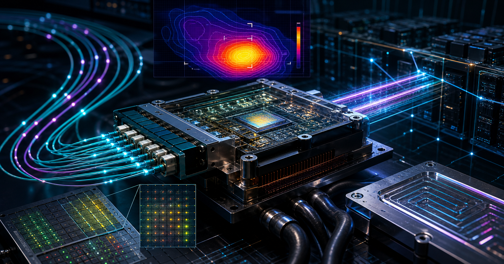
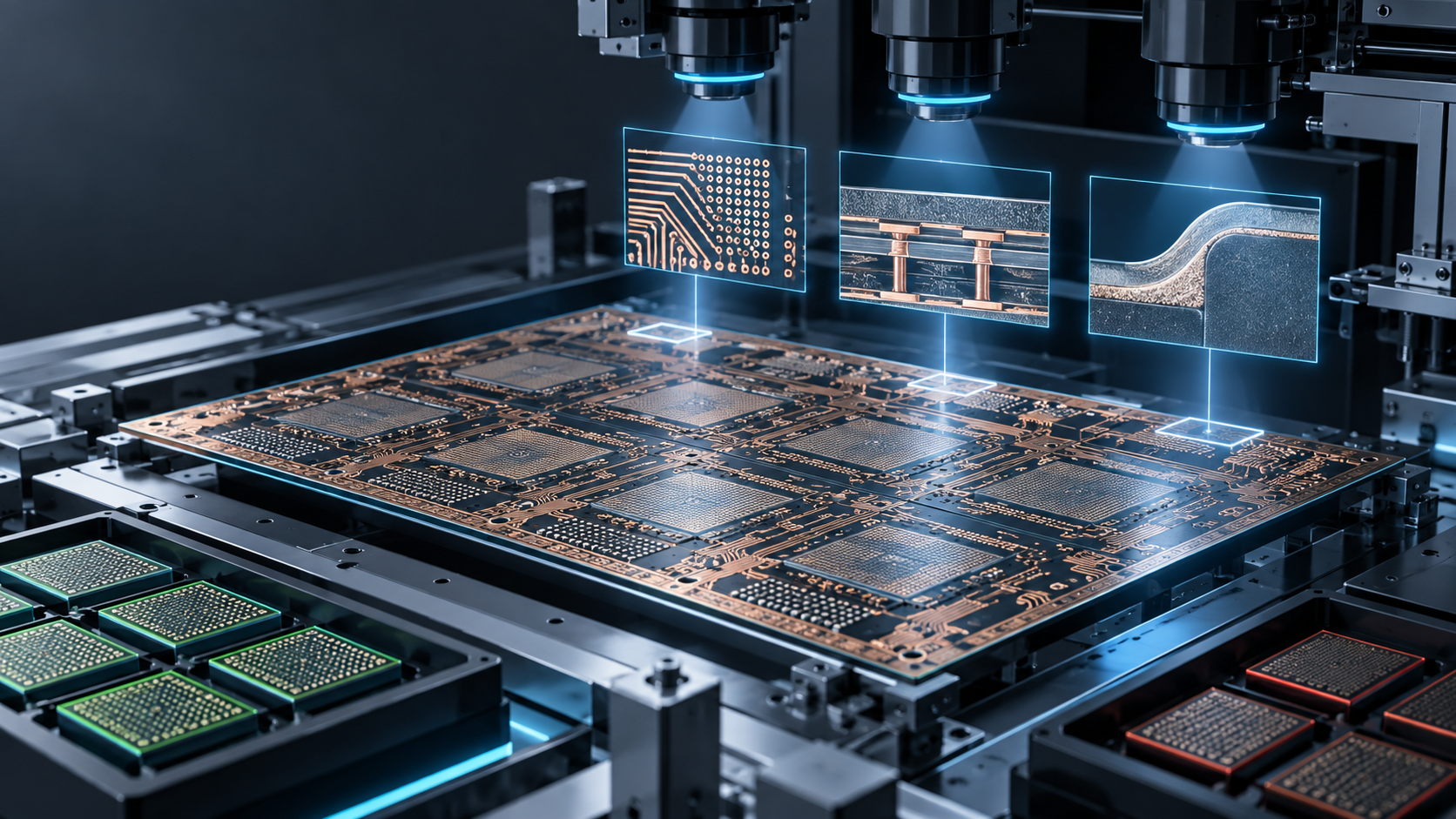
Elephantech is often summarized as a company that “prints copper with inkjet.” That description is directionally useful but no longer sufficient. Once the company’s disclosures through 2026 are placed in process order, copper nanoparticles perform different jobs in production FPC surface traces, HDI via walls, and semiconductor package substrates.
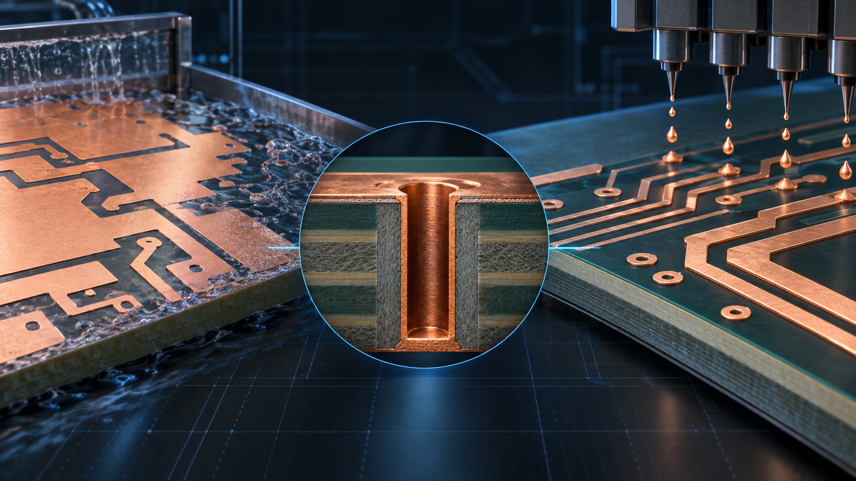
The direct answer is this: SustainaCircuits, which evolved from P-Flex, draws a copper foundation only where surface conductors are needed; DeepVia forms a plating seed on the walls of deep vias; and DS-SAP separates the seed requirements of the surface from those of the vias. Calling all three “printed wiring” blurs the line between a product already adopted in mass production and process technologies still undergoing customer evaluation.
The previous substrate overview lined up a group of companies — Elephantech, Absolics, Eliyan, Ayar Labs, and Panmnesia. This article takes one part of that picture, copper interconnect manufacturing, and reads it from the outside. It answers the more specific search intent—where Elephantech changes copper interconnect manufacturing and what “mass production” currently means—using only process details and evidence visible in official material. It does not fill undisclosed market size, yield, customer count, or financial figures with estimates.
Note: this piece is an outside-in read based solely on public information — company releases, product pages, papers, and press coverage.
Verification date: September 14, 2026. Company releases are primary sources for the company’s claims, not independent audits of complete production lines. Every number below is labeled as a company disclosure, an article calculation, or a scenario.
TL;DR: Four Points to Keep Straight
| Question | Answer |
|---|---|
| Is it one technology? | Copper nanoparticles, ink formulation, and inkjet control are shared assets, but the target process step differs |
| What has production evidence? | SustainaCircuits FPC has a disclosed mass-production adoption in a Logitech product |
| What remains at evaluation stage? | DeepVia HDI and DS-SAP have test results or customer evaluations, but no disclosed production yield or shipment volume |
| What matters for an investment view? | Track equipment delivery, customer qualification, repeat orders, material consumption, and yield after the technical demo |
Keeping these categories separate prevents a common inference: that because the company manufactures one product at volume, every newer process is already production-qualified.
Decomposing the Three Process Families
The most useful distinction in the source material is not the copper nanoparticle itself. It is where copper is placed and what function it serves.
Elephantech’s materials page describes copper nanoparticles with an average size of about 15nm and a D50 of 13.4nm. Ink stability, sinterability, substrate adhesion, and a primer that controls droplet landing and trace shape form a common technology base. The flows to the finished interconnect are nevertheless different.
| Family | Where the nanoparticle copper goes | Subsequent step | Stage supported by official material |
|---|---|---|---|
| SustainaCircuits FPC | Surface circuit pattern on the substrate | Copper plating grows the conductor to target thickness | In production since 2020; disclosed mass-production adoption in Logitech MX Vertical in 2025 |
| DeepVia HDI | Inner wall of an HDI via | Reduction creates a continuous film, followed by electrolytic copper plating | Prototype AR range of 3–4; 1,000 temperature-cycle pass in an August 2026 update; multiple evaluations underway |
| DS-SAP | Insufficient seed regions inside package-substrate vias | Combined with an independently formed ultra-thin surface seed and pattern plating | Cross-section for a 25μm-bottom-diameter via; evaluation by AI semiconductor and advanced-packaging companies |
SustainaCircuits grows surface conductors from selected locations
A subtractive flow begins with copper across the surface and removes the unwanted portion. SustainaCircuits prints copper nanoink on a primer only where a circuit is required, then grows conductor thickness by plating. In April 2025, the company claimed 70–80% less copper use than conventional methods. It described production of FPC conductors up to 100μm thick, development capability up to 200μm, and expansion beyond the existing 3–12μm range.
The 70–80% figure belongs to the company’s stated product and assessment boundary. It is not a universal factor for every trace density or layer stack. The MX Vertical adoption is evidence of product-level mass production, but the release does not disclose adopted area, unit price, or annual volume.
DeepVia replaces the seed-formation step on via walls
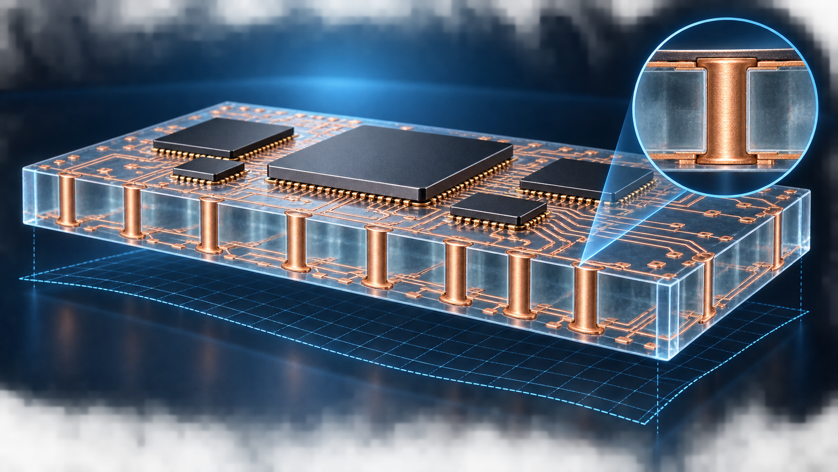
The December 2025 Cu Nano Direct Plating flow adsorbs copper nanoparticles onto desmeared via walls, uses a reduction treatment to create a continuous copper seed, and then applies electrolytic plating. In the disclosed test, a four-layer HDI vehicle with a 0.1mm top via diameter, 0.06mm dielectric, and 20μm target plating passed 700 cycles between −65°C and 125°C, with 15 minutes at each extreme and resistance variation within ±10%.
DeepVia HDI extended the disclosed range in April 2026 through a self-wetting ink for high-aspect-ratio structures. The company compares a conventional electroless-copper range of AR 1.0–1.2 with DeepVia at AR 3–4. Its August 2026 reliability update reports a 0.1mm bottom diameter, 0.2mm dielectric, 20μm target plating, 1,000 cycles between −55°C and 125°C with 15-minute dwells, and resistance variation within ±5%. Because the test vehicles and criteria differ, the move from 700 to 1,000 cycles is not a valid percentage performance improvement.
DS-SAP separates surface and via requirements
In a conventional SAP flow, surface and via seeds are formed together. A thicker surface seed increases removal time and conductor loss, which works against fine lines. A seed that is too thin, however, can leave discontinuities at the via bottom. DS-SAP places an ultra-thin electroless-copper or PVD seed on the surface and selectively supplements only the via with copper nanoink.
It would be inaccurate to describe this as filling the via with ink. The official cross-section shows seed supplementation, followed by electroplating, in an ABF GL-102 structure with a 25μm via-bottom diameter. The ink is not the entire final conductor fill. At announcement, multiple AI semiconductor and advanced-packaging companies had begun evaluations; production qualification and yield were not disclosed.
Reproducing the Copper-Material Arithmetic
When an environmental claim is expressed as one percentage, I prefer to start with a geometry-only model rather than applying the company figure to unrelated boards.
The article calculation assumes one square meter of a single layer, 18μm copper thickness, and copper density of 8,960kg/m³. Full-area copper mass is 161.28g. If the final conductor covers 30%, 50%, or 70% of the area, the theoretical amount removed by a subtractive flow is as follows.
| Final conductor coverage | Copper left in the traces | Theoretical removal from full foil | Removal ratio |
|---|---|---|---|
| 30% | 48.38g | 112.90g | 70% |
| 50% | 80.64g | 80.64g | 50% |
| 70% | 112.90g | 48.38g | 30% |
The calculation is reproducible with the same Python used in the Japanese section.
COPPER_DENSITY_KG_M3 = 8_960
AREA_M2 = 1.0
THICKNESS_M = 18e-6

full_foil_g = COPPER_DENSITY_KG_M3 * AREA_M2 * THICKNESS_M * 1_000

for coverage in (0.30, 0.50, 0.70):
    final_g = full_foil_g * coverage
    removed_g = full_foil_g - final_g
    print(coverage, round(final_g, 2), round(removed_g, 2))
This does not “validate” the company’s 70–80% reduction claim. Additive processing still has seed material, plating baths, edge losses, defects, washing, and rework; subtractive processing may recover copper. The narrow result is that trace coverage alone moves theoretical removal between 30% and 70%. A useful environmental or cost comparison therefore needs matched layer count, panel utilization, finished copper thickness, recovery rate, and good-unit yield.
Aspect ratio needs the same discipline. A 300μm dielectric divided by a 100μm via diameter gives AR 3.0; 200μm divided by 100μm gives AR 2.0. The company’s DeepVia range of 3–4 is roughly 2.5 to 4 times the disclosed conventional range of 1.0–1.2, but that is a geometric capability comparison. It does not imply the same multiple in line throughput or production yield.
Converting Technical Releases into Production Evidence
For an investment case, separating the maturity of the evidence is more useful than ranking novelty.
| Evidence stage | Example observed here | Information still needed | What it does not establish |
|---|---|---|---|
| Material and mechanism | About 15nm copper particles, primer, self-wetting behavior | Storage stability, lot variation, sintering window | High-yield production |
| Coupon or test vehicle | 25μm via cross-section; 700- or 1,000-cycle tests | Sample size, failure distribution, additional stresses | Full product lifetime |
| Customer evaluation | Multiple evaluations for DeepVia and DS-SAP | Qualification completion and equipment acceptance | Confirmed orders or revenue |
| Product mass production | FPC adoption in Logitech MX Vertical | Adopted area, duration, expansion to other products | Production status of the new via processes |
Pitfall: “mass production” refers to three different layers
The first is material production. The 2025 release says a stable production process exists for the copper nanoink, but that does not mean an HDI line at a customer is qualified. The second is production of Elephantech’s FPC product, for which Logitech is concrete adoption evidence. The third is deployment of equipment and consumable material into customer factories. Equipment acceptance and repeat material orders—not the existence of an FPC factory—will matter most to the future economics of DeepVia or DS-SAP.
A second pitfall is calling a reliability-test pass “yield.” Temperature-cycle resistance is meaningful evidence, but panel-wide via distributions, defect density, takt time, and maintenance frequency are separate variables. Filling those gaps with an industry average would create a precise-looking but unverifiable model.
Investment call: separate technical progress from the monetization path
Elephantech is not a directly investable listed equity as of this review, so this article makes no valuation call. The adopted view is to verify continuity of production FPC adoption in the near term and whether the equipment-plus-material model becomes repeatable at customer sites over the medium term. The rejected view is to infer revenue scale or profit contribution to listed companies solely from the start of AI-related evaluations.
Even when considering read-throughs to listed suppliers or prospective customers, I would not add a financial figure until the contracting party, revenue recognition, and unit economics are disclosed. The same discipline used in the AI semiconductor startup comparison framework and the back-end value-chain checklist applies here: contracts and production data have to bridge “technically needed” and “financially valuable.”
Scenarios and a Watchlist Through 2027
The least demanding central hypothesis is that FPC products and via-oriented equipment/materials will progress at different speeds.
| Scenario | Assumption | Evidence to watch | Condition that changes the view |
|---|---|---|---|
| Base case | FPC adoption expands while DeepVia / DS-SAP remain in evaluation | Continuity of current adoption and new test vehicles | Evaluation dates repeatedly slip without qualification |
| Main scenario | Customer deployment begins with bundled equipment and ink | Equipment delivery, acceptance, repeat material orders | Throughput or yield fails at a customer process |
| Upside | A package-substrate use reaches production qualification | Qualification completion, production application, supply capacity | Dependence remains concentrated in one customer or use case |
| Tail risk | Reliability, maintenance, or cost delays adoption | Specification changes, delivery delays, added evaluations | Multiple independent customers adopt under comparable conditions |
Five measurements would materially improve the analysis: good-panel yield, the defect distribution by via diameter and AR, equipment takt time, ink consumption and replacement frequency, and elapsed time from customer qualification to repeat order. Those data would move the discussion from interesting nanoparticles to production capability and unit economics.
The conclusion is intentionally bounded. SustainaCircuits FPC has product-level production evidence. DeepVia has condition-specific reliability evidence. DS-SAP has process cross-sections and customer-evaluation evidence. The latter two still lack disclosed mass-production yield and shipment volume. Holding that line is the shortest route to avoiding both underestimating and overclaiming Elephantech’s progress.
Related articles
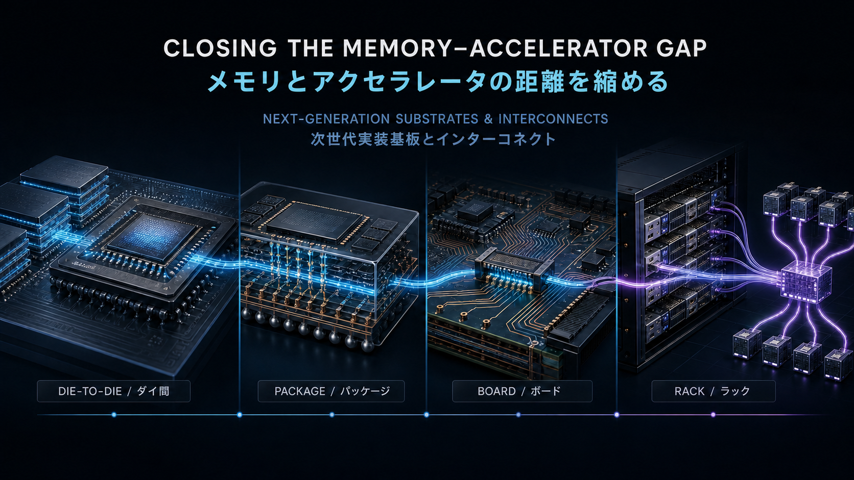
- Substrate technologies that close the distance between memory and accelerators — Maps whether a technology changes package, board, or rack-scale distance.
- A comparison framework for AI semiconductor startups — Connects technical performance to customer adoption and business evidence.
- The memory back-end value chain — Tracks substrates, bonding, and test through production disclosures.
Next Issue Ideas
- Idea 1: A production-readiness checklist for fine-via formation — Compare via diameter, AR, thermal cycling, and panel yield across several approaches under matched conditions.
- Idea 2: How seed formation changes on glass and ABF — Use primary sources to compare PVD, electroless copper, and copper nanoink on step coverage and interface reliability.
- Idea 3: Repeat revenue in PCB equipment businesses — Track equipment sales, ink consumables, and service revenue using disclosed contracts rather than assumed attach rates.
References
- Elephantech: Copper nanoparticles, inks, and primer technology
- Elephantech: Thin- and thick-copper SustainaCircuits FPC production, April 9, 2025
- Elephantech: Mass-production adoption in Logitech MX Vertical, April 21, 2025
- Elephantech: Cu Nano Direct Plating and the 700-cycle test, December 23, 2025
- Elephantech: DeepVia HDI AR range and 1,000-cycle test, April 24, 2026, updated August
- Elephantech: DS-SAP process and customer evaluations, June 18, 2026
This article is for informational purposes and is not a recommendation to buy any listed or private security. The author may hold securities issued by companies mentioned here or related companies. Generative AI assisted research, drafting, and translation. Calculations use stated assumptions and do not guarantee product performance, production yield, or investment returns. See the full disclaimer.