Closing the Distance Between Memory and Accelerators: What Elephantech, Absolics, and Eliyan Reveal About the Next-Generation Substrate
A field guide to what implementation substrates must deliver as memory and accelerators are pushed closer together, using Elephantech, Absolics, and Eliyan as concrete cases across package, board, and rack scale.
A field guide to what implementation substrates must deliver as memory and accelerators are pushed closer together, using Elephantech, Absolics, and Eliyan as concrete cases across package, board, and rack scale.


Closing the Distance Between Memory and Accelerators: What Elephantech, Absolics, and Eliyan Reveal About the Next-Generation Substrate
Note: this piece is an outside-in read based solely on public information — company releases, product pages, papers, and press coverage.
What does Elephantech change in substrate manufacturing? For semiconductor package substrates, DS-SAP forms the copper seed layers on the surface and inside vias separately, targeting fine traces alongside reliable via coverage. The official June 18, 2026 announcement reports customer evaluations but provides neither production yield nor volume-adoption counts. Development, evaluation, and production should be assessed separately.
The distinction among production FPCs evolved from P-Flex, DeepVia for HDI vias, and DS-SAP for package substrates is developed in a process-by-process follow-up on Elephantech's copper interconnect technology, including a reproducible copper-material calculation.
The short answer to the glass-core search intent is that lower-warpage material properties do not establish manufacturability. A follow-up comparing TGV, warpage, and panel yield at matched evidence stages separates test vehicles, pilot lines, and volume production using primary Intel, NIST, Samsung Electro-Mechanics, and Corning material plus a reproducible scenario calculation.
For a cross-technology production decision, use the five-level framework for customer qualification, step yield, equipment acceptance, and repeat orders.
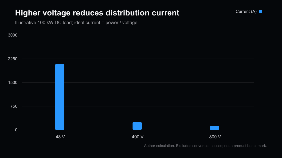
For the complementary question of delivering power to the rack, see the 800V distribution, GaN and SiC roles, and current and efficiency comparison.
September 17, 2026 update: The opening answer and DS-SAP process wording were checked against official material, and contextual links were added to the Elephantech and glass-core manufacturing follow-ups. Other company information retains the original verification date below. This update was automated and is not represented as human-reviewed.
Back when I was developing automotive EEPROM process technology, I ran into the same failure mode over and over right before volume production: board warpage going haywire during reflow and dragging yield down with it. Trace the cause far enough and it almost always came back to a small mismatch in coefficient of thermal expansion (CTE) between the die and the package material. My routine at the time was to run structural simulations in ANSYS or Autodesk Fusion 360, map out where stress concentrated across a thermal cycle, and then fix the mold and the layer stack-up before it ever hit the line. Reading through the news on Absolics' glass-core AI substrate and Elephantech's new process for semiconductor package substrates for this piece, I kept thinking: this is the same fight, just several orders of magnitude bigger in scale and money.
Last time, I wrote about d-Matrix and TetraMem and how they close the distance between memory and compute inside a single die. This time I want to move one layer outward — to the space between chips: the implementation substrate, the package, and the board. If d-Matrix and TetraMem are attacking the wall inside the die, the companies in this piece are attacking the wall outside it — the package substrate, the printed circuit board, and the wiring inside a rack. It's the same "memory wall," but the battlefield changes, and so does what actually counts as a winning move.
Version note: Product, procurement, and shipment status is as of August 17, 2026, drawn primarily from company announcements and trade-press coverage. Performance figures and investment amounts are vendor-reported or press-reported and should not be read as guarantees of future results or as directly comparable across companies.
TL;DR: What You'll Learn
| Topic | What you'll learn |
|---|---|
| The distance hierarchy | "Distance" splits into four layers, from sub-1mm die-to-die connections to meter-scale rack fabrics |
| Rebuilding the substrate itself | Elephantech's additive copper printing and Absolics' glass-core substrate attack the same problem with different materials and processes |
| Making the connection smarter | Eliyan's die-to-die PHY aims to match interposer-class bandwidth and power without an interposer |
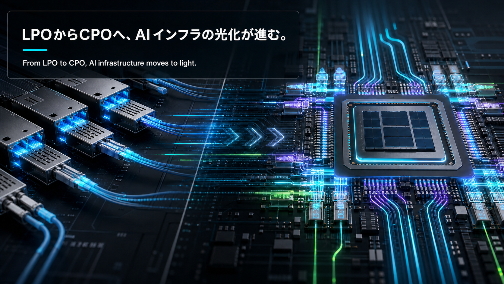
| Giving up on distance, using light | Ayar Labs' co-packaged optics (CPO) solves rack-scale distance with light instead of copper |
| Capital momentum | Elephantech, Absolics, and Ayar Labs alone have pulled in hundreds of millions to billions of dollars in 2026 |
Breaking the "Memory Wall" Down as a Distance Problem
My conclusion up front: the memory wall isn't one wall. It's four walls of different character, stacked by distance.
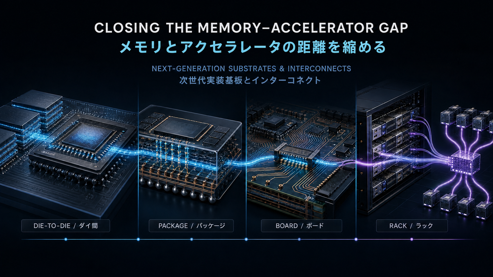
When an AI accelerator reads or writes weights, the signal doesn't just travel inside the die — it crosses the package, the board, and in some cases cables inside a rack. Each segment has different capacitance, resistance, and power-cost characteristics. Die-to-die connections (2.5D interposers, hybrid bonding) run under 1mm; package substrates run tens of millimeters; chip-to-chip traces on a printed circuit board run centimeters; rack-level wiring runs meters. Every order-of-magnitude jump in distance changes both the materials in play and the design philosophy needed to handle it.
My point in this piece is simple: the tidy slogan "close the distance between memory and accelerators" hides four genuinely different questions — which layer's distance, closed by which method. One company physically thins and refines the substrate itself to shrink distance. Another eliminates an entire intermediate layer — the interposer — to make distance disappear from the bill of materials. A third gives up on shrinking distance altogether and escapes into a different physical medium: light.
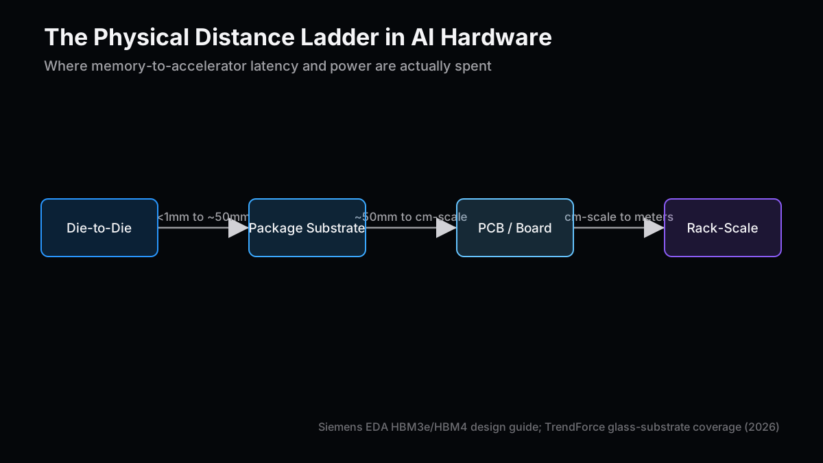
Laid out as four tiers, it looks like this.
| Tier | Representative distance | Primary technology | Representative players |
|---|---|---|---|
| Die-to-die | Under 1mm | 2.5D silicon interposer, hybrid bonding | TSMC CoWoS, Eliyan NuLink |
| Package substrate | Tens of mm | Organic ABF substrate, glass-core substrate, additive wiring | Absolics, Elephantech |
| PCB / board | Centimeter scale | Multilayer PCB, fine-pitch routing | Elephantech (general-purpose PCB) |
| Rack-scale | Meter scale | CXL fabric, co-packaged optics (CPO) | Panmnesia, Ayar Labs |
Before deployment, it helps to have a rough sense of how distance maps onto energy cost, so you don't misdiagnose which layer's problem you're actually looking at. Instead of a full signal-integrity analysis, I use a deliberately crude model like this as a first conversation starter.
# Rough mapping from physical distance to interconnect tier
# (order-of-magnitude only; real design points vary by generation)
TIERS = [
    (1.0, "die-to-die (2.5D interposer / hybrid bonding)"),
    (50.0, "package substrate (organic ABF / glass core)"),
    (500.0, "board-level (multilayer PCB, additive fine-pitch)"),
    (float("inf"), "rack-scale (CXL fabric or co-packaged optics)"),
]


def interconnect_tier(distance_mm: float) -> str:
    for limit, label in TIERS:
        if distance_mm <= limit:
            return label
    raise ValueError("unreachable")


def relative_energy_cost(distance_mm: float, pj_per_bit_per_mm: float = 0.15) -> float:
    # Energy roughly tracks trace length once a channel is electrically long;
    # this is a first-pass gut check, not a signed-off SI budget.
    return distance_mm * pj_per_bit_per_mm
This code doesn't substitute for real signal-integrity work. What it does do is instantly sort a piece of news into "this is a die-to-die story," "this is a substrate story," or "this is a rack story." In HBM4 terms: JEDEC standardized HBM4 in April 2025 with a 2048-bit interface across 32 independent channels, delivering over 2.0TB/s per stack (up to 3.3TB/s in advanced configurations), and volume production ramped through early 2026. In a CoWoS-style 2.5D configuration, the silicon interposer routes HBM-to-processor connections at sub-2-micron line/space, across a distance of just a few millimeters — a completely different world from a DDR module running tens of centimeters across a printed circuit board.
Rebuilding the Substrate Itself: The Process and Material Bets Behind Elephantech and Absolics
The two companies in this section are attacking a classic problem — routing copper — from angles that have almost nothing in common.
Elephantech: Print the Copper Instead of Cutting It Away
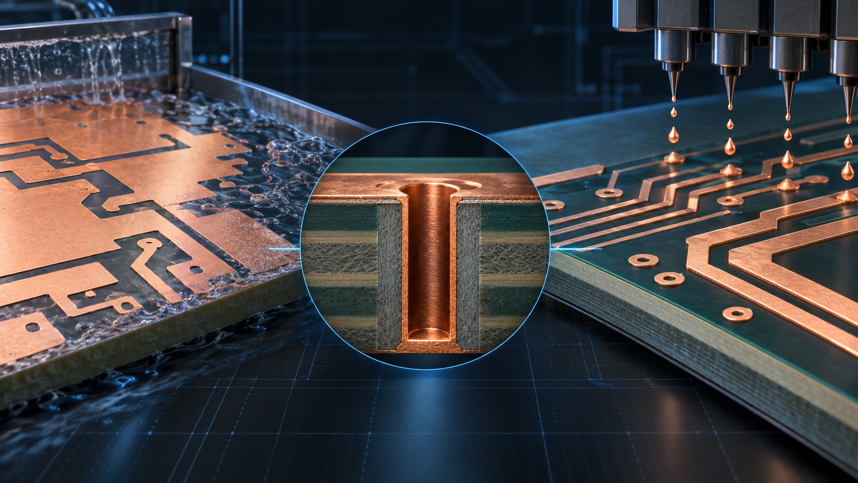
Tokyo-based Elephantech is known for SustainaCircuits, a proprietary additive wiring process. Conventional PCB manufacturing is dominated by a subtractive process: you laminate copper foil onto a base material, then etch away everything you don't need, discarding most of the copper as waste. SustainaCircuits inverts that. It inkjet-prints copper nanoparticle ink only where a circuit is actually needed. According to the company, this cuts copper consumption by 70% and CO2 emissions by 75% versus the conventional process.
On March 12, 2026, Elephantech announced a ¥4 billion (roughly $27M) Series F from Mitsubishi Electric. The stated purpose is straightforward: scale up mass-production capacity for the SustainaCircuits inkjet equipment and accelerate adoption among PCB manufacturers worldwide. The global PCB market is estimated at roughly ¥10 trillion, and the partnership pairs Mitsubishi Electric's industrial-equipment manufacturing and support know-how with Elephantech's nanomaterial and inkjet expertise to go after a slice of the general-purpose multilayer PCB segment.
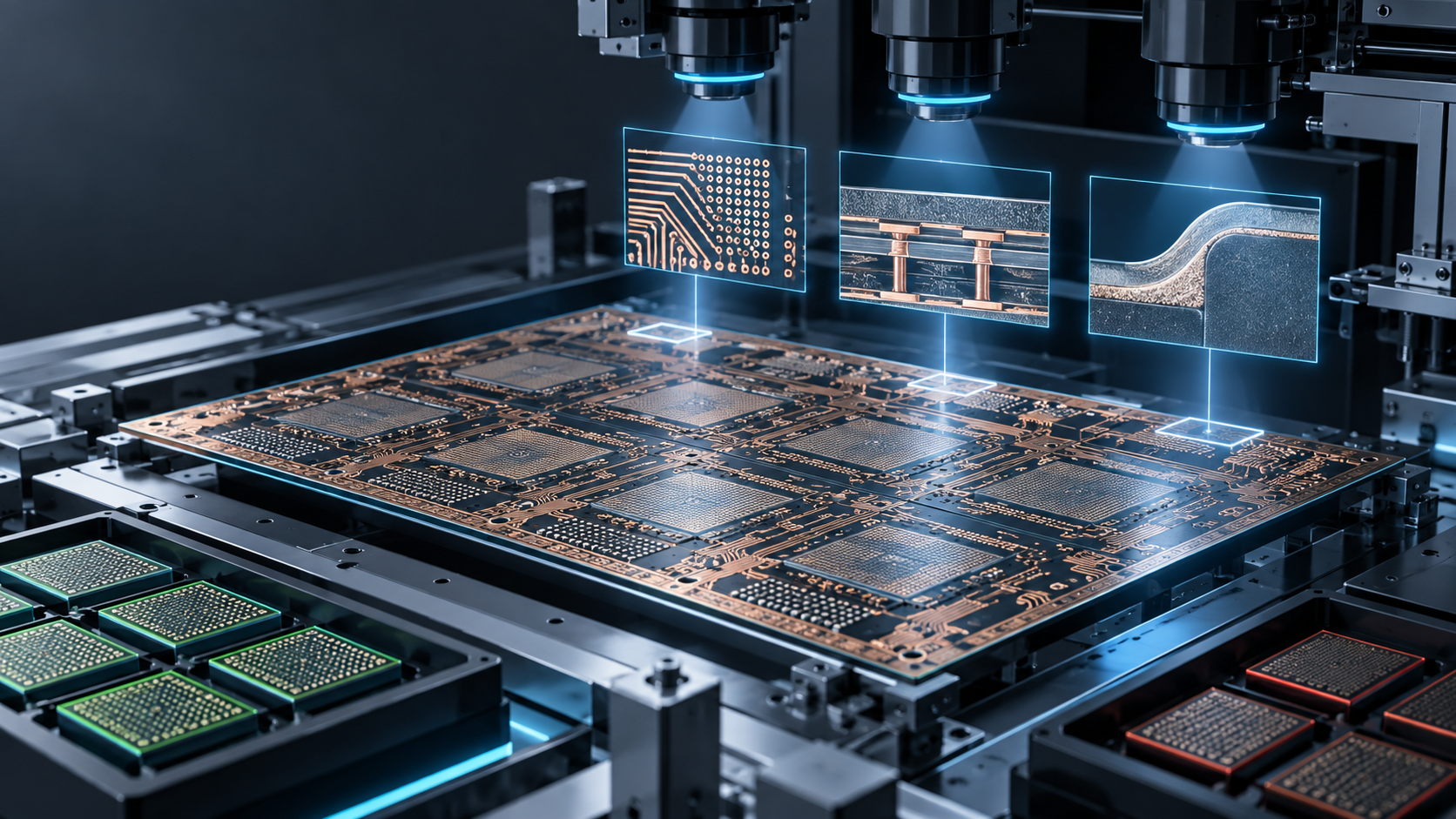
What surprised me most while researching this piece was DS-SAP (Dual-Seed Semi Additive Process), announced June 18, 2026. It's a process built specifically for semiconductor package substrates, and it targets a real trade-off in conventional semi-additive processing: you want an ultra-thin seed layer on the surface for fine patterning, but you also want thick, reliable seed coverage inside high-aspect-ratio vias — and conventional processes struggle to give you both at once. DS-SAP splits seed-layer formation into two independent stages: an ultra-thin surface seed via electroless copper plating or PVD, followed by copper nanoparticle ink applied to the vias to complete insufficient seed-layer coverage. The company has published demonstration data on 25-micron-diameter vias, and says it has begun evaluations with several AI semiconductor manufacturers and advanced-packaging companies.
Absolics: Betting on Glass as the Substrate That Doesn't Warp
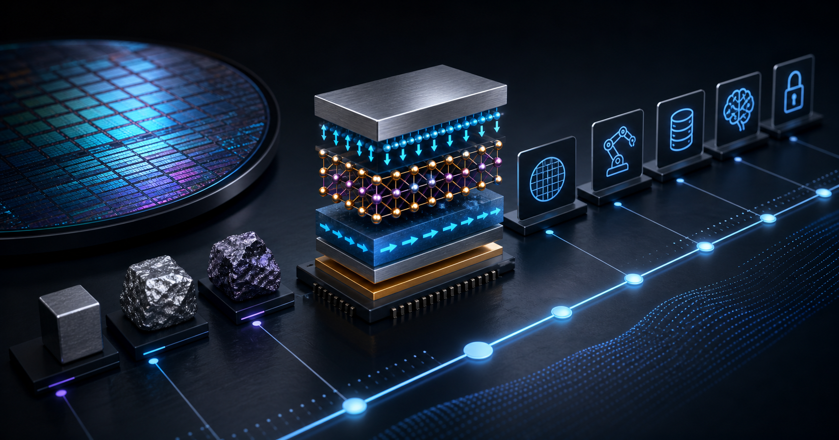
Absolics — an SKC subsidiary roughly 30%-owned by Applied Materials — took a completely different angle. Instead of an organic ABF substrate, its inProut platform uses glass as the core material.
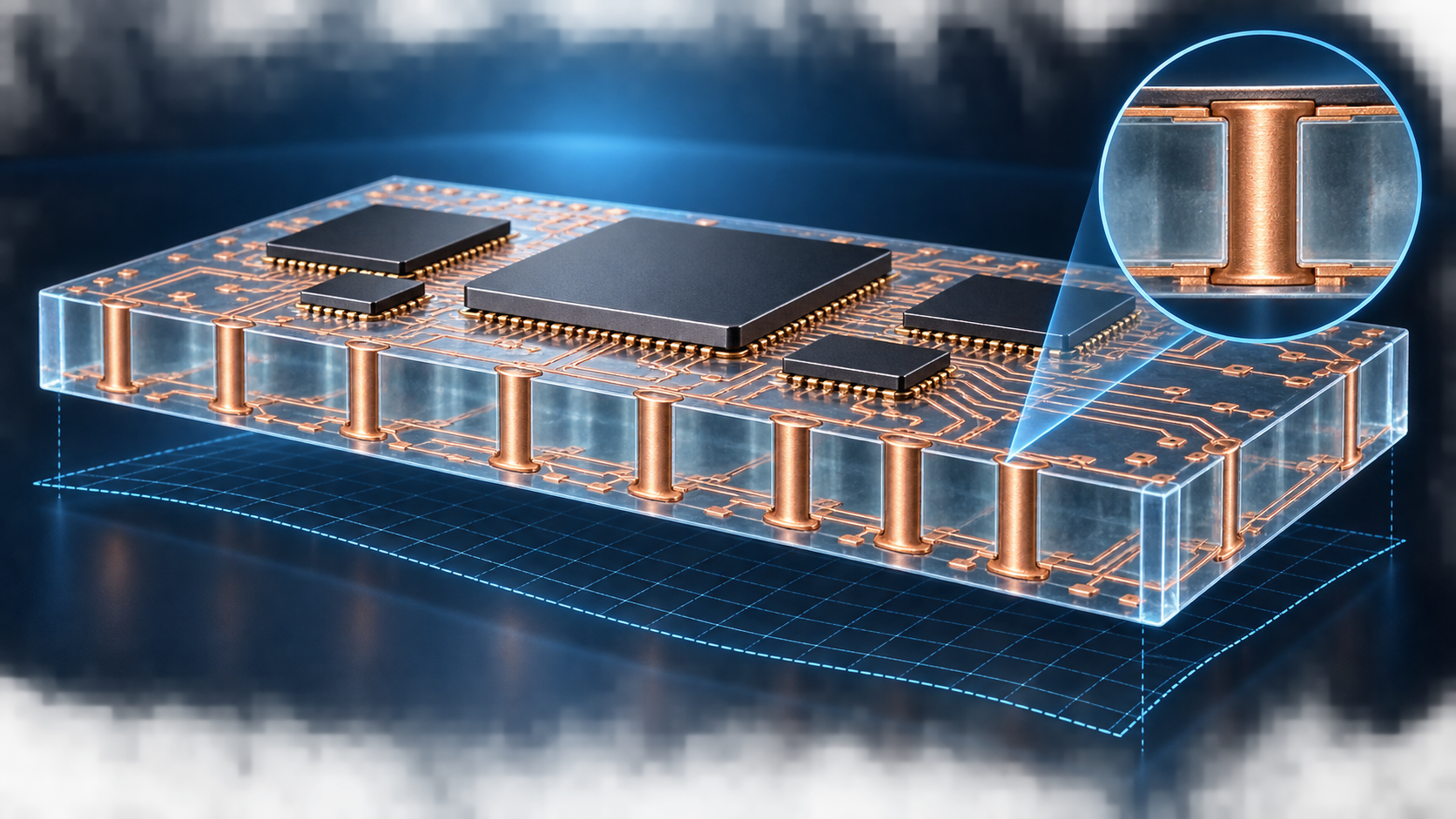
This is where my EEPROM-era experience comes back into play directly. Organic substrates expand and contract at a different rate than a silicon die (a CTE mismatch), and the bigger the package gets, the more that mismatch shows up as warpage you can't ignore. What I spent a good chunk of my process-development years chasing during reflow was exactly this: how a CTE mismatch between die and substrate concentrates stress, and where. Glass has a CTE much closer to silicon's, and unlike a round silicon wafer, it can be processed as a large rectangular panel — so in principle, you can build a bigger, thinner, more finely routed substrate while keeping warpage under control. My first reaction to "why glass, of all things" was skepticism. Once you factor in CTE mismatch as a physical constraint rather than a footnote, though, the choice makes a surprising amount of sense.
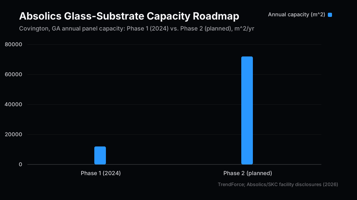
Absolics has drawn $75M in manufacturing support (May 2024) and $100M in R&D support (December 2024) from the US CHIPS Act to build out its Covington, Georgia facility, reportedly a roughly $600M investment. As of January 2026, the company had begun shipping volume-production-grade samples for AMD's MI400-series accelerators, with supply to Amazon reportedly underway as well. A "Phase 2" expansion is in progress to grow annual panel capacity sixfold, from 12,000 to 72,000 square meters.
Glass substrates still carry real, practical downsides: they're more fragile and currently more expensive than the alternative. The industry consensus is that 2026 is the "high-end adoption" year, reserved for AI accelerators priced above $20,000, with broader adoption into workstation and gaming markets not expected until around 2028. Elephantech and Absolics are targeting different layers (general-purpose PCB versus AI-accelerator package substrate) and betting on different materials (how you print copper versus the substrate material itself) — but both are pointed at the same underlying shift: turning the substrate from a passive supporting actor into an actively engineered part of the system.
| Item | Elephantech (SustainaCircuits / DS-SAP) | Absolics (inProut glass core) | Conventional organic substrate (ABF) |
|---|---|---|---|
| Base material | Resin substrate + additive copper wiring | Glass core | Organic resin (ABF film) |
| Process | Inkjet copper nanoparticle printing + plating/PVD | Glass panel processing + fine via formation | Subtractive / semi-additive processing |
| Layer it targets | General-purpose multilayer PCB, fine wiring on semiconductor package substrates | Package substrates for large AI accelerators | Package substrates broadly |
| Strength | 70% less copper, 75% less CO2, fine + reliable via coverage together | Low warpage, large-format panels, fine wiring density | Proven track record, mature cost and supply chain |
| Challenge | Full production-line adoption is still ahead | Fragility and cost, ramping production yield | Warpage becomes dominant as packages scale up |
| Status as of 2026 | Evaluations underway with AI semiconductor makers (DS-SAP) | Volume samples shipping for AMD MI400-class | Running as the mainstream default |
Rebuilding the Die-to-Die Connection: How Eliyan's NuLink Makes the Interposer Optional
Instead of rebuilding the substrate, Eliyan chose a third path: engineer the interconnect smart enough that you can skip the expensive interposer altogether.
Eliyan's NuLink PHY is a die-to-die interconnect IP that supports two industry standards — UCIe (Universal Chiplet Interconnect Express) and BoW (Bunch of Wires) — across a wide range of bump pitches from 40 to 130 microns. After an early test chip on TSMC's 3nm process, the latest generation, NuLink-2.0, taped out on Samsung Foundry's SF4X (4nm) and hits 64Gbps per bump — which Eliyan describes as the industry's highest die-to-die PHY performance. The explicit target is HBM4-class memory.
I ran into a simple doubt here: can you really eliminate the interposer entirely? That sounded almost too convenient. Reading the spec more closely, though, the claim turns out to be narrower and more defensible than the headline suggests. NuLink-SP (the Standard Packaging variant) lets a design fit up to 4x more HBM stacks into a single package while running on an ordinary organic substrate. Because it removes the dependency on interposer readiness, it cuts packaging, test, and assembly costs by at least 2x and shortens time-to-market by up to 26 weeks. The real claim, in other words, is "match interposer-class bandwidth and power efficiency on a standard package, without an interposer" — not "no design ever needs an interposer again." Within the range where that claim holds, though, an entire layer of the packaging stack simply disappears from the bill of materials.
| Item | NuLink-2.0 (advanced bump pitch) | NuLink-SP (standard packaging) |
|---|---|---|
| Supported bump pitch | 40-130 microns | Fits standard organic substrate assembly tolerances |
| Bandwidth per bump | 64Gbps (3nm process) | Targets interposer-class bandwidth/power efficiency |
| Effect on HBM capacity | - | Up to 4x more HBM stacks in the same package |
| Effect on cost / lead time | - | Packaging/test cost cut by 2x+, lead time shortened by up to 26 weeks |
This also changes how you should read the HBM4 standard itself. JEDEC's HBM4 spec defines the physical signal; whether that signal travels through a silicon interposer or through a NuLink-class PHY on a standard package is a design decision that sits outside the standard. Part of the race to close distance has quietly shifted from "physics of the substrate" to "cleverness of the interconnect IP."
Giving Up on Distance and Escaping to Light: Ayar Labs' CPO and the Push to Rack Scale
The first three companies were all fighting over millimeters. At rack scale — meters — the physics changes entirely.
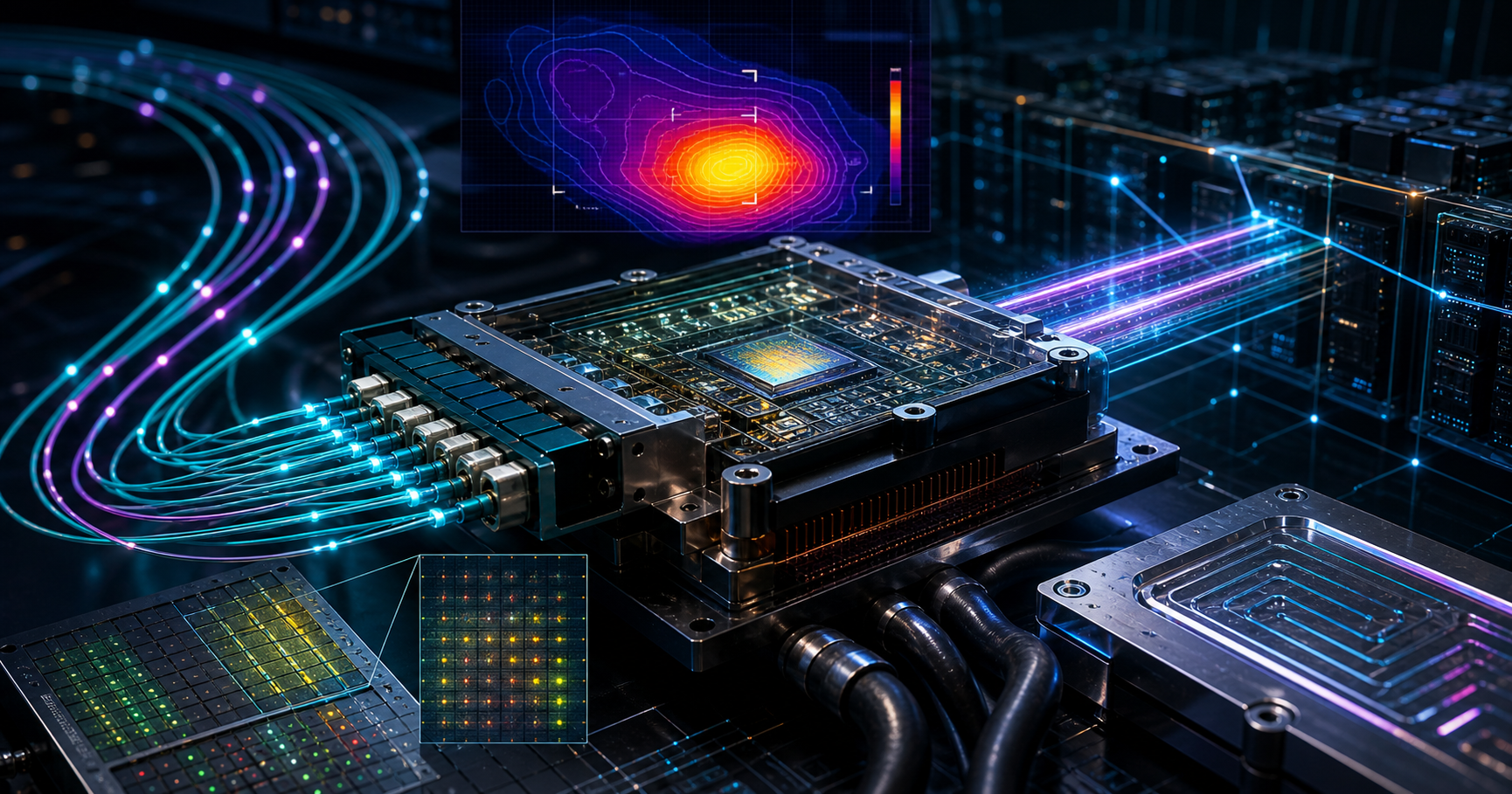
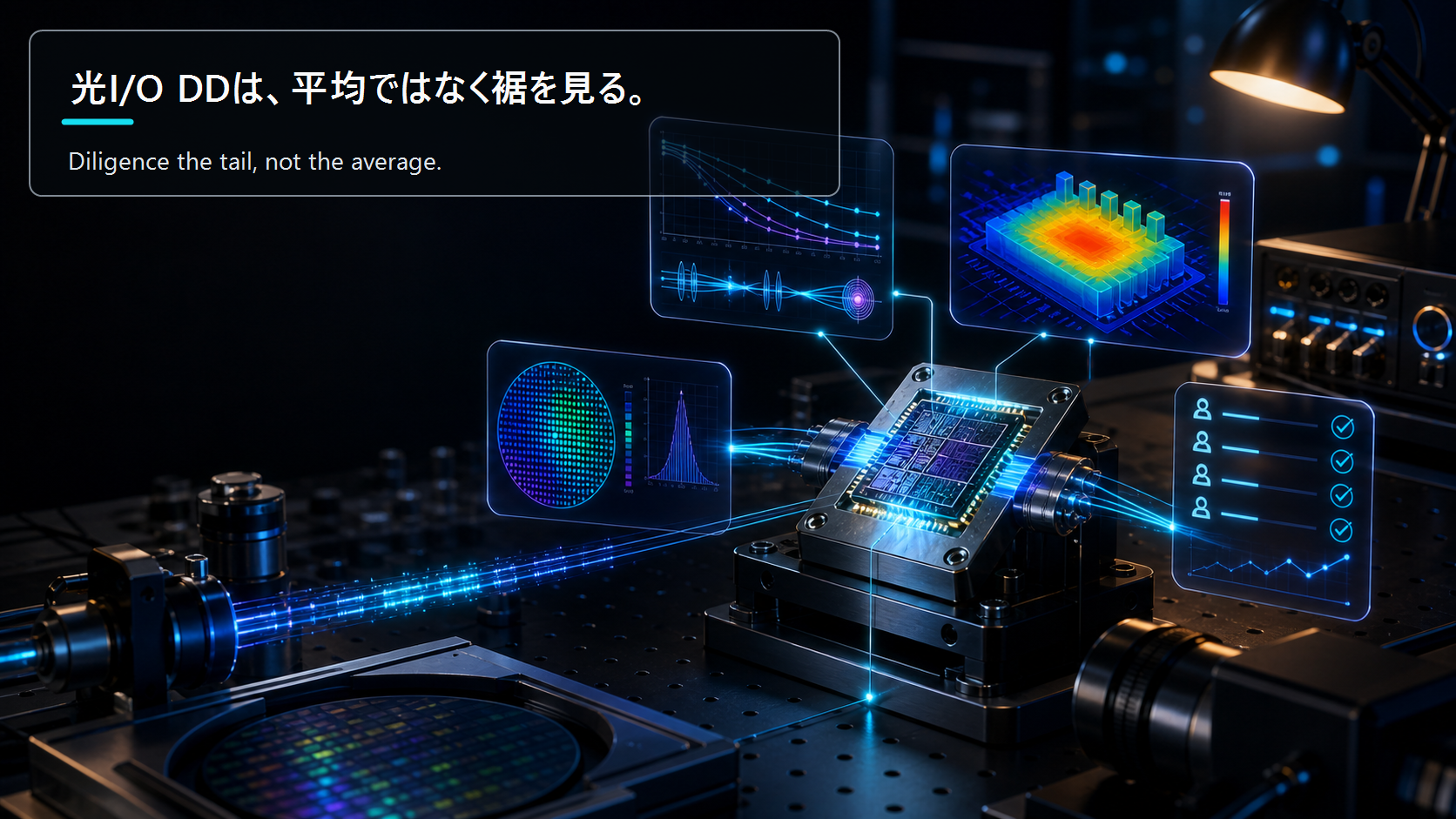
Copper attenuation gets exponentially worse with distance, so trying to cover meter-scale runs with electrical signaling alone forces you into repeaters and complex equalization, and power consumption climbs fast. Ayar Labs' co-packaged optics (CPO) carries that segment with light instead, which means it doesn't play the "loss scales with distance" game at all. This extends a line of argument I covered previously in a framework for reading optical I/O startups and in a piece on CPO ramp yield and thermal design.
On March 3, 2026, Ayar Labs closed a $500 million Series E led by Neuberger Berman, bringing total funding to roughly $870 million at a $3.75 billion valuation. The investor list runs from ARK Invest, Insight Partners, the Qatar Investment Authority, Sequoia Global Equities, and 1789 Capital to strategic backers AMD, Alchip, MediaTek, and NVIDIA. Reading that list, I take the fact that both upstream and downstream players in semiconductors are all writing checks as a signal that the industry has stopped treating CPO as "an interesting technology" and started treating it as infrastructure that belongs in the supply chain.
In November 2025, Ayar Labs partnered with Taiwanese ASIC design house GUC to integrate its optical engines into advanced-packaging and ASIC design flows. At OFC in March 2026, it announced a rack-scale reference design with ODM partner Wiwynn that stitches together more than 1,024 GPUs into a single system — fully liquid-cooled, HVDC-powered, using ELSFP SuperNova remote light sources.
What I find most interesting here is that CPO takes the exact opposite stance on distance from Elephantech and Absolics. Elephantech and Absolics physically rebuild the substrate to shrink distance itself. Ayar Labs gives up on shrinking distance and escapes into a medium — light — where distance-driven loss is close to a non-issue. Both are ultimately chasing the same goal — move data between memory and accelerators faster and cheaper — but they've picked opposite strategies to get there.
Pushing the Scale Outward: Panmnesia and the Question of Whether Memory Belongs on the Same Die at All
The last company on this list, Panmnesia, poses a slightly different question than the other four.
South Korean fabless startup Panmnesia builds switch silicon and IP centered on CXL (Compute Express Link). It raised a Series A of over $60M at roughly a $250M valuation in November 2024, bringing total funding across three rounds and 17 investors to about $102M. In 2025, it was selected for a $30M government-backed project to redesign AI datacenter architecture around chiplets, manycore designs, processing-in-memory (PIM), and CXL. Early 2026 brought an additional $10M government R&D project targeting direct chip-to-chip interconnects between AI accelerators, and in April 2026 the company announced a PCIe 6.4-compatible CXL 3.2 Fusion Switch sample chip.
Here I want to push back on my own framing for a moment. Does pooling memory over CXL and sharing it across multiple accelerators actually "solve" the distance problem? Or does it just push a physical constraint behind a layer of software abstraction? Thinking it through, both answers are partly right. A CXL fabric doesn't make the electrical distance 1mm. But it removes the constraint that memory has to sit physically next to one specific accelerator in the first place, and replaces it with pooling and allocating capacity wherever it's actually needed. Just as Eliyan redefines the distance problem by removing an intermediate layer — the interposer — Panmnesia asks an even more upstream question: does this memory need to sit on the same die or package at all?
I sort companies along a "shrinking distance" versus "nullifying distance" axis when I build technology synergy maps for investment cases, and this is exactly why. Elephantech and Absolics sit on the shrinking-distance side; Ayar Labs and Panmnesia sit on the nullifying-distance side; Eliyan sits right in the middle. All five wave the same "memory wall" banner, but the questions worth asking as an investor differ completely depending on where a company actually sits.
What Performance Substrates Must Deliver, and Where Development Goes Next
Plot all five companies on a single map and this is what you get.
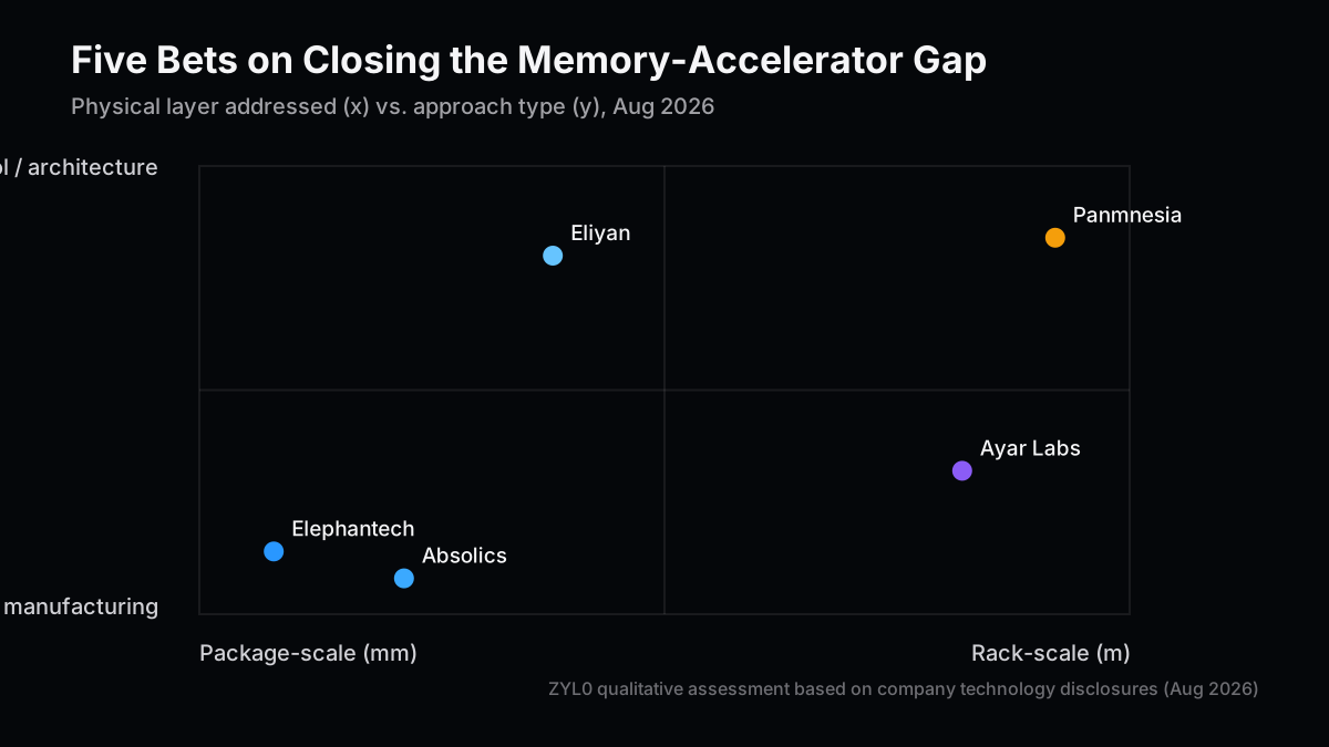
The x-axis runs from package scale to rack scale; the y-axis runs from material/manufacturing innovation to protocol/architecture innovation. Elephantech and Absolics sit in the lower-left (package scale x material innovation); Eliyan sits toward the upper-left (package scale x protocol innovation); Ayar Labs sits toward the lower-right (rack scale x innovation in the physical medium itself); Panmnesia sits in the upper-right (rack scale x architecture innovation). Capital is flowing into every quadrant of this map at once.
| Company | Recent funding | Valuation / scale indicator |
|---|---|---|
| Elephantech | Series F, ¥4B (Mitsubishi Electric, March 2026) | Undisclosed |
| Absolics | $175M combined CHIPS Act support (2024), ~$600M Covington facility | Undisclosed (SKC subsidiary) |
| Eliyan | Undisclosed (primarily technology licensing to semiconductor makers) | Undisclosed |
| Ayar Labs | Series E, $500M (March 2026, ~$870M total raised) | $3.75B valuation |
| Panmnesia | Series A $60M+ plus ~$40M in government-backed projects | ~$250M valuation |
Three directions for development follow from this map, as I read it.
First, substrate materials keep diversifying. Glass core, additive wiring, and conventional organic ABF will settle into different niches based on cost-versus-performance trade-offs, rather than one material winning outright. As of 2026, glass substrates are confined to AI accelerators priced above $20,000 — not every workload needs a frontier substrate.
Second, interconnect IP starts to reshape the packaging decision itself. As technology like Eliyan's matures, "should this design use an interposer" turns into a continuous cost-versus-performance trade-off rather than a binary default, and designers get to choose project by project whether to shrink distance physically or nullify it with a smarter connection.
Third, the distance problem keeps expanding outward — from the package to the rack, and from the rack to the data-center architecture as a whole. CPO and CXL fabrics are redefining the relationship between memory and accelerators, from "fixed next-door neighbor" to "pooled capacity, connected by light, allocated on demand."
The performance metrics that matter for implementation substrates shift accordingly: line/space (microns), via aspect ratio, panel/wafer scalability, warpage and CTE matching, bandwidth density (GB/s per mm²), energy efficiency (pJ/bit, or GB/s per watt), and cost and time-to-volume. No single substrate optimizes all of these at once. Even a single metric like HBM3's rated 141.2 GB/s/W — three times GDDR5's throughput at roughly a fifth of the power — is the product of substrate, package, and interconnect all advancing together, not any one layer working in isolation.
Gotchas: Discount Substrate-Vendor Claims Before You Act on Them
The single riskiest habit in a packaging-and-substrate article is comparing numbers from different contexts as if they belonged on the same scale.
- Demos are not production: DS-SAP's 25-micron via demonstration and NuLink's 64Gbps-per-bump figure are both measured results under specific conditions — neither guarantees production-line yield.
- "No interposer needed" is a scoped claim: What Eliyan's NuLink-SP eliminates is the interposer within a specific bandwidth and capacity range, not every HBM configuration.
- Press-reported investment figures aren't final: Numbers like Absolics' Covington facility investment shift depending on context — whether subsidies are included, whether multiple phases are combined.
- Glass substrates are still a niche: As of 2026 they're confined to AI accelerators above $20,000, and won't go mainstream until the cost structure changes.
- CPO and CXL solve different distance bands: Ayar Labs' CPO addresses rack scale; Eliyan's NuLink addresses package scale. Comparing them head-to-head as "which is better" misses the point.
- Where this framing does not fit: For cost-first edge devices with modest bandwidth needs, or designs that a conventional organic substrate already handles comfortably, the investment case for the frontier substrates and interconnects covered here doesn't transfer directly. If memory bandwidth isn't the actual bottleneck, pushing to a more advanced substrate buys little return.
When I spot an eye-catching number in a vendor's release, my first move is to look for the conditions under which it falls apart. In substrates and packaging, that level of skepticism is about the right dose.
Closing: The Technology That Shrinks Distance and the Technology That Gives Up on It Share One Map
Having written all this out, I keep coming back to how closely the warpage fight from my EEPROM years mirrors what these five companies are doing today. Back then, I was chasing a CTE mismatch between die and package material, bouncing between simulation and physical measurement to find an answer. Elephantech, Absolics, Eliyan, Ayar Labs, and Panmnesia are, at a wildly different scale of money and stakes, solving the same underlying problem — how to make peace with physical constraints — at different layers, with different tools.
There's no single correct answer to closing the distance between memory and accelerators. Some companies change the substrate material. Some remove an intermediate layer with smarter interconnect IP. Some give up on distance and escape into light. Some try to make the whole concept of "distance" irrelevant. As both an investor and an engineer, I think the first job is correctly sorting which layer, and which kind of distance, a given story is actually about. Get that right, and the measured numbers will do the rest of the talking.
Next Issue Ideas
- Idea 1: Tracking HBM4 Production Yield — Checking TSV and Hybrid-Bonding Data Against Disclosures — Cross-compare yield trends at SK Hynix, Samsung, and Micron as HBM4 moves from JEDEC standardization into early volume production.
- Idea 2: Decomposing the Glass-Substrate Cost Curve — When Do Absolics and Intel's Production Curves Cross? — Track the glass-substrate cost curve from 2026's "high-end only" phase toward broader adoption around 2028.
- Idea 3: Actually Measuring CXL Memory Pooling — Finding the Break-Even Point for Panmnesia-Style Architecture on Latency and TCO — Test, at an implementation level, how much added latency a CXL-fabric memory access can tolerate compared to local HBM.
Related Posts
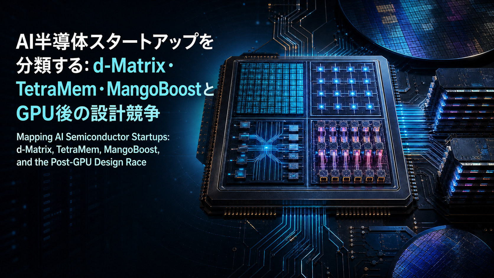
- Mapping AI Semiconductor Startups: d-Matrix, TetraMem, MangoBoost, and the Post-GPU Design Race — The layer just inside this one: closing the memory wall within a single die.
- How to Read Optical I/O Startups From the Outside: Insertion Loss, Thermals, Manufacturability, and Customer Validation — A practical framework for reading CPO companies like Ayar Labs from public information.
- The Real CPO Ramp: Winners in AI Data Center Optics Through Yield and Thermal Design — A deeper look at rack-scale optical conversion through yield and thermal design.
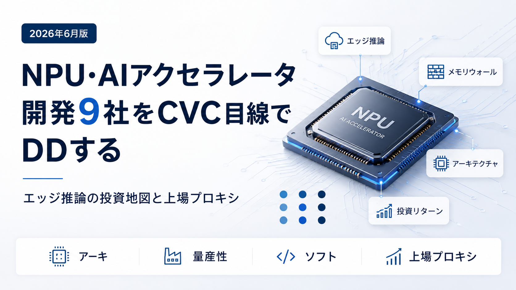
- Reading the 9 NPU / AI-Accelerator Developers From the Outside: An Edge-Inference Investment Map and Its Public Proxies — An outside-in map of the architectural splits driving the memory-wall debate.
- The Memory Squeeze Runs to 2031: How Samsung 70 Percent Lock-Up Rewires HBM Supply and the Back-End Value Chain — The follow-up: how contract lock-up reprices supply and pushes profit toward the back end.
References
The figures and facts in this post are anchored to the following sources readers can verify (as of August 17, 2026).
- Elephantech: Mitsubishi Electric Invests in Elephantech Under New Partnership
- Elephantech: DS-SAP™ for Fine Patterning on Semiconductor Package Substrates
- Absolics Inc.: Glass Substrate (inProut)
- TrendForce: Glass Substrates Are Breaking Through the AI Chip Packaging Bottleneck
- Eliyan: NuLink Technology
- Ayar Labs: Ayar Labs Closes $500M Series E, Accelerates Volume Production of Co-Packaged Optics
- Insight Partners: Ayar Labs Closes $500M Series E
- Design & Reuse: CXL Fabless Startup Panmnesia Secures Over $60M in Series A Funding
- Siemens EDA: HBM3e and HBM4 IC Design Guide
This article is for informational purposes only and does not constitute investment advice or a recommendation to buy any specific stock, company, product, or service. Performance figures, investment amounts, and valuations are vendor-reported or press-reported and do not guarantee comparability across companies or future results. Generative AI was used for parts of the research, translation, and proofreading. The additions and corrections dated September 13, 2026 were automated. See the disclaimer for details.