How to Read Optical I/O Startups From the Outside: Insertion Loss, Thermals, Manufacturability, and Customer Validation
An outside-in checklist for reading optical I/O startups from public information: insertion loss, thermals, manufacturing yield, and customer validation, all under volume conditions.
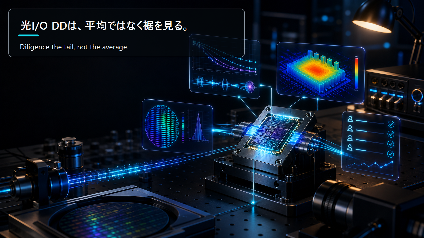
An outside-in checklist for reading optical I/O startups from public information: insertion loss, thermals, manufacturing yield, and customer validation, all under volume conditions.


How to Read Optical I/O Startups From the Outside: Insertion Loss, Thermals, Manufacturability, and Customer Validation
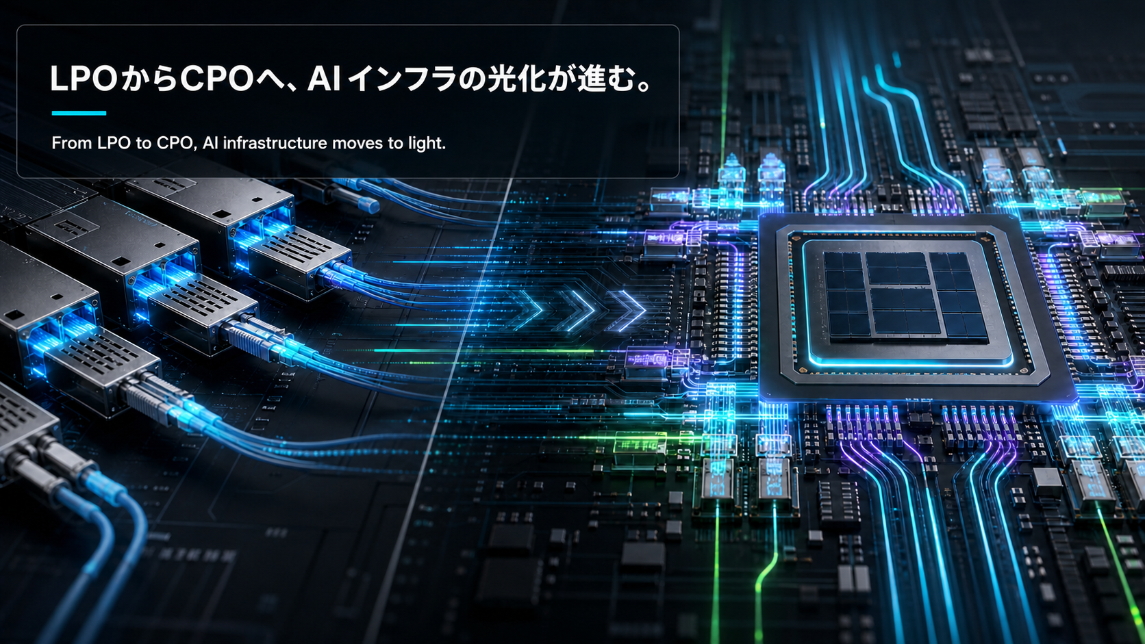
At the end of the previous post (the LPO vs CPO migration map), I listed "how to read optical I/O startups" as the second next-issue idea. This piece pays off that promise. In the earlier post (the real CPO ramp) I argued that the real CPO contest is yield and thermals, and in the migration map I concluded that the medium-term positions live in CPO sub-assembly and PIC foundries. So when you look at a startup in that space from the outside, which pieces of public information do you read, in what order, and with which numbers? This post is that checklist.
Note: this piece is an outside-in read based solely on public information — company releases, product pages, papers, and press coverage.
I came up through semiconductor process engineering, worked on automotive EEPROM volume production, and once used TCAD to find the real root cause of a yield failure that had been reported as "an equipment problem." Later I moved to CVC, where I found that the investment team had no unified quality bar for investment reviews and built one. Optical I/O looks like an "optical communications" theme, but to my eye it is a combined advanced-packaging, thermal, and test problem. Do not get hypnotized by the clean charts in a release — read insertion loss, thermals, manufacturability, and customer validation under volume conditions. That is the whole argument. This is a May 2026 snapshot, and the numbers will move within six months.
Why Optical I/O Startups Are Won or Lost on How You Measure
Let me open with an observation: optical I/O announcements are frequently technically right and investably wrong. The reason is simple. The published numbers are best-unit, lab-condition data, and what I want to know is the tail of the volume distribution.
Optical I/O startups split into two broad lineages. There are CPO sub-assembly players (the assembly shops that build optical engines, external lasers, and fiber attach) and there are architecture/PIC-foundry players — names like Ayar Labs, Lightmatter, and Celestial AI. Both call themselves "optical I/O," but the pressure points to look at differ.
| Lineage | Representative private players | Source of value | Pressure point to look at |
|---|---|---|---|
| CPO sub-assembly | Private assembly shops, suppliers around Coherent/Lumentum | Assembly, alignment, yield | Volume yield and test capability |
| PIC foundry | GF Fotonix, TSMC COUPE, Tower (fabs) + private | Process and capacity | Process portability and PDK maturity |
| Optical I/O IP / architecture | Ayar Labs, Lightmatter, Celestial AI | Architecture and customer design-ins | Customer validation and volume transfer |
The easy mistake is conflating the technical question with the manufacturing question. The technical question is: does it work? The manufacturing question is: does it close on yield, thermals, and cost? Optical I/O companies pass the former and fail the latter far more often than not. This post leans hard into the latter.
If I compress the whole picture into one table — the metric, how to measure it, and a 2026 pass line — it looks like this. The chapters that follow take one axis at a time.
| Evaluation axis | Key metric | How to measure | Rough 2026 pass line |
|---|---|---|---|
| Insertion loss | Coupling loss (dB/connection), link-budget margin | Volume-lot distribution, worst case, aging | Grating coupling < 2dB, edge coupling < 1.5dB, managed at 3σ |
| Thermals | Wavelength drift (pm/°C), TEC-less margin | Temp-cycle tests, real case temp near ASIC | Wavelength control holds at 80–90°C operation |
| Manufacturing / yield | Engine yield, KGD, test coverage | Lot-to-lot variance, yield learning curve | Engine yield > 60–70%, improving quarter over quarter |
| Customer validation | Design-in count, certification stage, PO/NRE | Customer seniority, contract form, exclusivity | On a third-party hyperscaler's eval board |

Axis 1: Insertion Loss and Link Budget — Read the Tail and the Aging, Not the Average
The first gate for optical I/O is coupling. My observation is that the numbers published here are, almost without exception, best units. I do not look at the average. I look for whether the tail of the distribution and the aging behavior are disclosed.
Insertion loss is unglamorous, but it drives the entire link budget. Add and subtract transmit power, coupling loss, fiber loss, and detector sensitivity, and what matters is how many dB of margin survive at the end. In CPO that margin is thin, and an extra 0.5dB of coupling loss flows straight into power consumption or bit error rate. When I wrote in the earlier post that "coupling shift raises insertion loss and raises power," this is precisely the mechanism.
| Metric | Good sign | Red flag | What I want to see |
|---|---|---|---|
| Coupling loss (median) | Grating < 2dB / edge < 1.5dB | Only shows best units | Full distribution across volume lots |
| Coupling loss (worst / 3σ) | Within +1dB of median | "We don't track the worst case" | Tie it to the yield acceptance criterion |
| Aging | < 0.5dB rise over thousands of hours | No accelerated-test data | Raw temp/humidity and powered-life data |
| Alignment method | Passive alignment in production | Active-alignment dependence, long takt | Per-unit assembly takt and yield |
| Polarization / wavelength dependence | Flat across band | Optimized only at one wavelength | Loss distribution across the volume wavelength spread |
The configuration I am most wary of is active-alignment dependence. Active alignment delivers precision, but because each unit has to be powered up and walked into position, takt time stretches and cost runs wild at volume. A company whose yield stands up under passive alignment — meeting spec through mechanical mating — is far stronger in production. In my EEPROM days, the more "tune-in" steps a product carried, the more its yield swung lot to lot. The same structure shows up in optical I/O.
One more point. However good the median coupling loss looks, if a meaningful fraction of lots throws 3σ worst-case units above the acceptance threshold, that fraction is pure yield loss. A company that speaks in averages usually cannot manage its tail. That is my rule of thumb.
Axis 2: Thermals — Wavelength Drift and the TEC Question Decide Cost and Reliability
A second observation: the essence of optical I/O thermals is not "can you cool it" but "can you hold the wavelength while the temperature swings?"
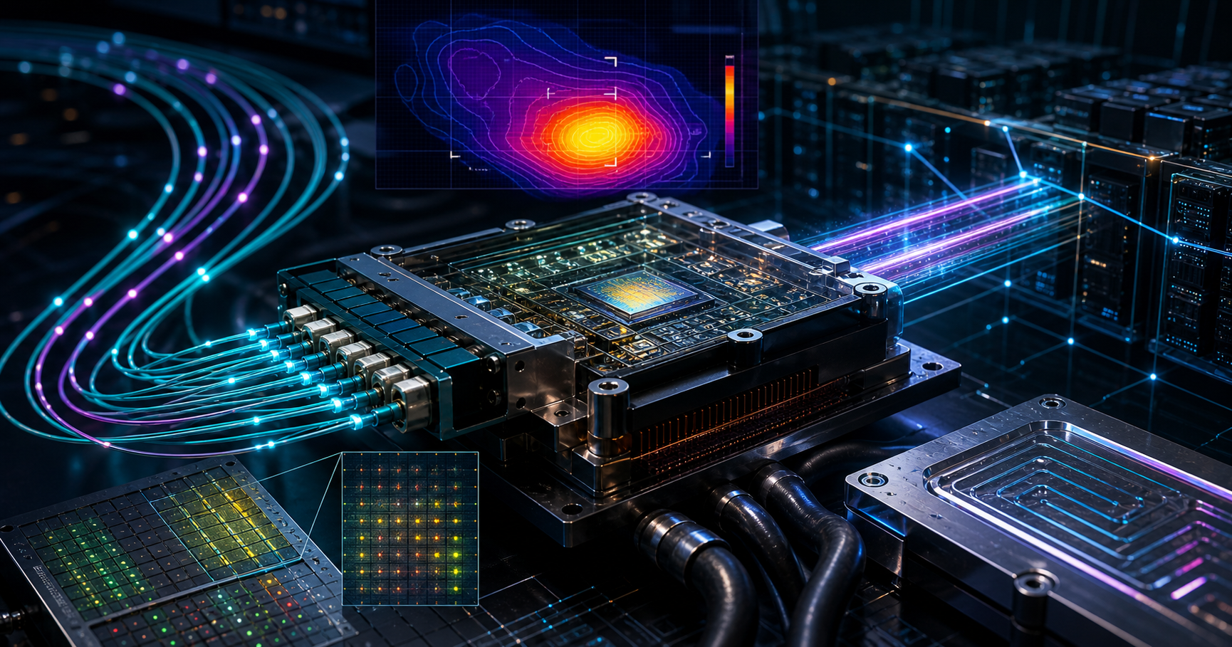
CPO places optical engines right next to a hot switch ASIC. Silicon-photonic modulators and ring resonators are temperature-sensitive, and their wavelength drifts with heat — typically on the order of tens to 100 pm/°C. This is where designs diverge. Either you actively pin the wavelength with a TEC (thermo-electric cooler) or heaters, or you chase a near-athermal design that needs no TEC. A TEC works, but it eats power and cost. A company that holds a wide temperature range without a TEC wins on both cost and reliability — I weight this heavily.
| Thermal topic | What to measure | Good sign | Red flag |
|---|---|---|---|
| Wavelength drift | pm/°C, residual error after control | Wide range held TEC-less | TEC assumed, control power undisclosed |
| Operating temperature range | Real case temp near the ASIC | Link held at 85–90°C | Room-temperature data only |
| Thermal cycling | Loss rise after -40 to 125°C cycles | Stable over hundreds to a thousand cycles | No cycling test done |
| Laser thermal management | Stability of external lasers | ELSFP-style heat-source separation | Integrated laser, tight thermal coupling |
| Control power | W/engine for wavelength control | Low TEC/heater power | Control power eats the efficiency gain |
The key is that thermals must be read at the system level, not on a spec sheet. I wrote previously that heat density near the ASIC degrades optical-engine stability, but what startups publish is mostly room-temperature, standalone data. The data I look for is the case temperature when this sits on the ASIC package, and the residual wavelength-control error at that temperature. A company that has not shown it probably is not yet at the stage of publishing system-level validation.
Whether they use external lasers — the ELSFP philosophy of physically separating the heat source from the optical engine — is also a question. Integrated lasers win on integration density, but they put the most thermally fragile component, the laser, right next to the ASIC. I give credit to external-laser-plus-redundancy designs from a long-term reliability standpoint.
Axis 3: Manufacturing and Yield — KGD, Test Coverage, and Portability
The third axis is, to me, the heart of it. Optical I/O has a deep valley between "a working demo" and "volume."
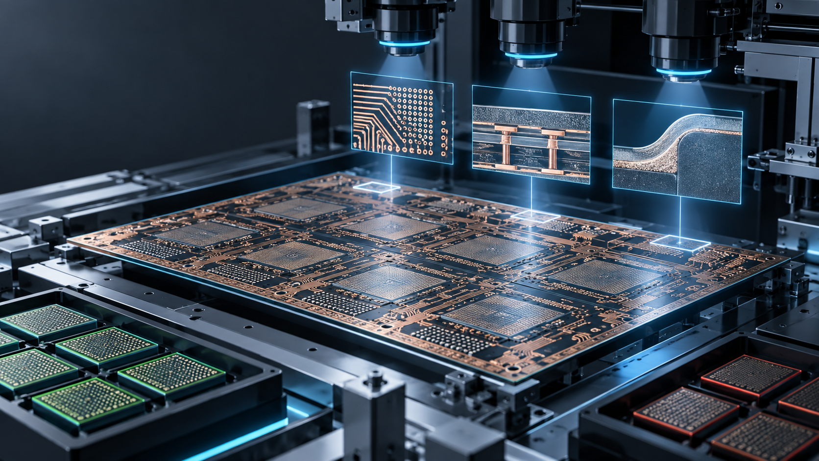
Because CPO pulls the optical engine inside the package, Known Good Die (KGD) — the ability to guarantee a good part before you place it — is decisive. In pluggables you swap a bad module; in CPO, placing one bad engine ruins the entire expensive ASIC package. So how completely you can co-test optics, electrical, and thermals before placement governs both yield and cost. Of the five failure modes I listed earlier (coupling shift, laser degradation, thermal drift, substrate warpage, inadequate test), it is the last one — inadequate test — that sits at the center of the manufacturing question.
| Manufacturing metric | How to measure | Good sign | Red flag |
|---|---|---|---|
| Engine yield | Recent-lot good rate and trend | Above 60–70% and improving | Only one best lot shown |
| KGD assurance | How a good part is judged pre-placement | Combined optical/electrical/thermal wafer/die test | Can only be judged after placement |
| Test coverage | Number of failure modes screened | Covers the main five failures | Electrical only, manual optical inspection |
| Yield learning | Improvement curve across lot sequence | Learning is climbing | Flat, root cause blamed on "equipment" |
| Process portability | Foundry / PDK dependence | Standard PDK, multiple foundries possible | Single-line custom dependence |
| Burn-in | Ability to weed out infant mortality | Simultaneous optical/electrical burn-in | No burn-in in place |
In my experience, the most eloquent signal is the yield learning curve. If the good rate climbs against lot sequence, there is a working loop that isolates and kills root causes. A company that stays flat while blaming the equipment is dangerous. I myself once used TCAD to prove that an EEPROM yield failure blamed on equipment was actually process variation interacting with another step. A company that cannot explain its yield has usually just not reached the real cause yet.
Portability cannot be skipped either. A custom process glued to a single line at a single foundry runs straight into capacity constraints at volume. That is what I meant in the migration map when I wrote that "12-inch PIC line capacity is the binding constraint." A design that rides a standard PDK and can transfer across multiple foundries — GF Fotonix, TSMC COUPE, Tower — is far better positioned for the scale phase.
Axis 4: Customer Validation — Read the Quality of a Design-in Through Seniority and Contract
The fourth axis is the most easily faked. My observation: "we're talking to a big customer" carries almost zero information. I look for what has been made public: with whom, at what stage, under what contract.
Optical I/O ultimately has to land on the eval board of a hyperscaler or switch-ASIC vendor or it means nothing. What matters is the design-in stage and the shape of the money tied to it — NRE, PO, exclusivity. MOUs and LOIs guarantee, in my book, essentially nothing.
| Customer signal | Weak | Medium | Strong |
|---|---|---|---|
| Who they talk to | Procurement / IR desk | Design engineer | Architecture lead |
| Stage | Intro / NDA | Eval board on loan | Design-in / certification in progress |
| Money | Free samples | NRE received | Volume PO, prepayment |
| Exclusivity | None | Preferred negotiation | Time-bound exclusive supply |
| Who validates | The startup itself | One customer department | Third-party lab, multiple customers |
What matters here is cross-checking the startup's claims against what the customer itself says: whether the same story shows up in the customer's press releases, earnings commentary, and conference talks. I once stood in an investment committee and, with data, flagged that a startup's claimed design-in progress did not match the customer's own understanding, then led the valuation renegotiation. Customer validation is confirmed in the customer's words, not the startup's.
You also have to understand the weight of certification. Optical I/O lives and dies on interoperability certification with switch ASICs (Broadcom Tomahawk, NVIDIA Spectrum, Marvell Teralynx families). Certification takes time, and once cleared it creates switching cost. A company with certification in progress is starting to build a moat even if the technology is a little rough — I add points here.
A Red-flag Master List — When This Combination Appears, Stop
Cutting across all four axes, here is the one-page list of triggers that make me pass or discount. Individually some are not fatal, but the danger of optical I/O is that several stack and correlate.
| Red flag | Why it is dangerous | What I want to see |
|---|---|---|
| Only best-unit numbers shown | Sign they cannot manage the volume distribution | The full distribution of the last three lots |
| Active alignment + high takt | Cost and yield run wild at volume | Per-unit assembly takt and yield |
| TEC assumed, control power undisclosed | The efficiency advantage may vanish | Wavelength-control power in W/engine |
| KGD "only judged after placement" | Yield loss drags down the expensive ASIC | How a good part is judged before placement |
| Flat yield + "blame the equipment" | Root cause not yet reached | The yield curve across lot sequence |
| Single foundry / custom dependence | Capacity constraint hits at scale | A standard PDK and a second source |
| Customer is MOU/LOI only | No money is moving | The real NRE, PO, and exclusivity terms |
| Room-temperature data only | System-level thermal validation incomplete | Residual error at the case temp near the ASIC |
My rule of thumb is that the most dangerous combination is "best-unit numbers + flat yield + customers are MOU-only." That is the classic pattern of technology that works but has neither volume nor a commercial channel — and it tends to inflate valuation with every funding round while nothing real moves. Conversely, when "speaks in distributions + climbing yield + NRE received" line up, I will lean in even if the technology looks unglamorous.
Scenario Analysis: Will Investing in This Segment Pay Off?
To close, here is a scenario frame for whether investing in CPO sub-assembly and PIC-foundry-class optical I/O startups pays off over 2026–2028. The previous post focused on the timing of the LPO-to-CPO handover. This one shifts the focus to the return distribution of positions selected on these four axes.
| Scenario | Subjective probability | Story | The type that benefits after four-axis selection |
|---|---|---|---|
| Base | 50% | CPO enters volume at 1.6T from late 2027; yield is the rate limiter | Sub-assembly that has proven volume yield + KGD |
| Bull (pulled in) | 20% | Hyperscalers pull CPO adoption forward | PIC/IP names with certification in progress + a second source |
| Bear (delayed) | 20% | Yield/thermals delay CPO; LPO life extends | Companies with TEC-less thermal design + test capability |
| Tail (redesign) | 10% | Heat/warpage forces a partial redesign | Companies strong in test, burn-in, and portability |
In the base case, the winner is not "the fastest light" but "the assembly shop that proves volume yield and KGD earliest." In the bull case, names with certification and a second source can withstand the pull-in; in the bear and tail cases, the unglamorous capabilities — test, thermals, portability — ironically hold the value. What works across every scenario is whether you read the four axes of this post under volume conditions. The thing that pays off independent of scenario is how deeply you read the manufacturing side — that is my conclusion.
The segment I currently see as most mispriced is the assembly players who can run KGD and inline optical inspection at volume. The market reads them as "subcontract assembly shops," but they are the first thing to choke in a CPO ramp and they are hard to substitute. Just like the retimer IP and fiber connectors I flagged last time, the structure holds for optical I/O too: the boring bottleneck gets priced during the volume phase.
The conclusion: optical I/O passes the technical question and fails the manufacturing one. Read insertion loss on the tail and aging, thermals on the TEC question and real system temperature, manufacturing on KGD and the learning curve, and customer validation on stage and contract. Only the companies that public information shows clearing all four axes under volume conditions get me leaning in. This is my view as of May 2026, and I will mark it to market in six months.
Next Issue Ideas
- Idea 1: The Liquid-cooling Bill of Materials for AI Data Centers — A Map of CDUs, Connectors, Coolants, and Sensors — Decompose the liquid-cooling BOM that ramps alongside CPO, component by component. The continuation of the "cooling periphery" thread left from posts 23 and 26, and directly contiguous with the thermal questions here.
- Idea 2: The Economics of Silicon Photonics IP Licensing — A Value-chain Analysis of PIC Foundries vs. IP Vendors — Compare the revenue models of private IP names like Ayar Labs, Lightmatter, and Celestial AI against the capacity economics of publicly traded PIC foundries — a deeper dive on the "portability" axis from this post.
- Idea 3: KGD and Test Economics in CPO Sub-assembly — Why a Single Point of Yield Moves Market Cap — A contrarian deep dive that quantifies KGD and inline optical inspection, the heart of the manufacturing question, through cost structure and valuation sensitivity.
Related Posts
- The Investment Map of AI Infrastructure's "Silicon Periphery": Power, Cooling, Optics, and Site Plays Hiding in Plain Sight — Watching only NVIDIA and AMD misses the point.
- The Real CPO Ramp: Winners in AI Data Center Optics Through Yield and Thermal Design — Optical conversion of AI datacenters is inevitable, but CPO mass production isn't just a bandwidth race.
- LPO vs CPO: The 2026–2028 Optical Interconnect Migration Map for AI Infrastructure — AI data center optics will arrive as a two-stage rocket — LPO first, CPO next.
- Semiconductor VC Series③: Designing for Volatility — Why Tier-1 VCs decompose semiconductor investing into "design productivity, data movement, packaging, supply chain" ra…
References
The factual and numerical assumptions in this article are anchored to primary or public materials that readers can revisit during AdSense review and future updates.
- OIF implementation agreements and CPO resources
- IEEE Photonics Society resources
- SIA semiconductor market data
This article is for informational purposes only and does not constitute investment advice or a recommendation of any specific stock, service, or contract structure. The author may hold positions or interests related to companies or services mentioned. Generative AI was used for parts of research, translation, and proofreading, with final review by ZYL0. See the disclaimer for details.