Will the University of Tokyo's Nonvolatile Quantum Switching Element Rewrite Semiconductor Investing? Key Names and the Timeline
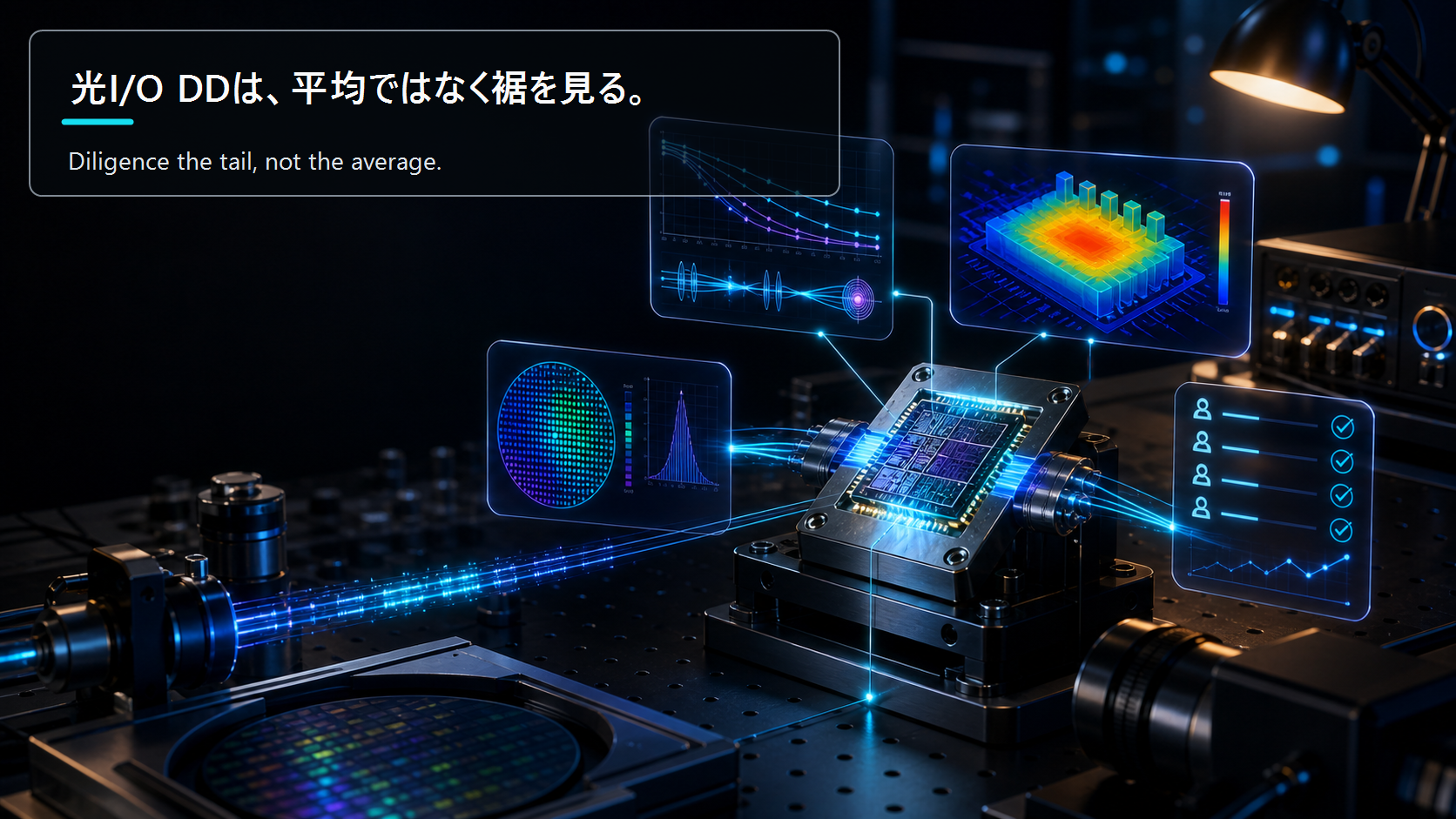
1000× faster, drastically less heat, 100 billion endurance cycles — UTokyo's May 2026 Science-published spin device targets a 2030 commercial trial. A CVC sorts material, equipment, and IP-holding tickers and maps second-order ripple effects into edge AI / robotics across time horizons.
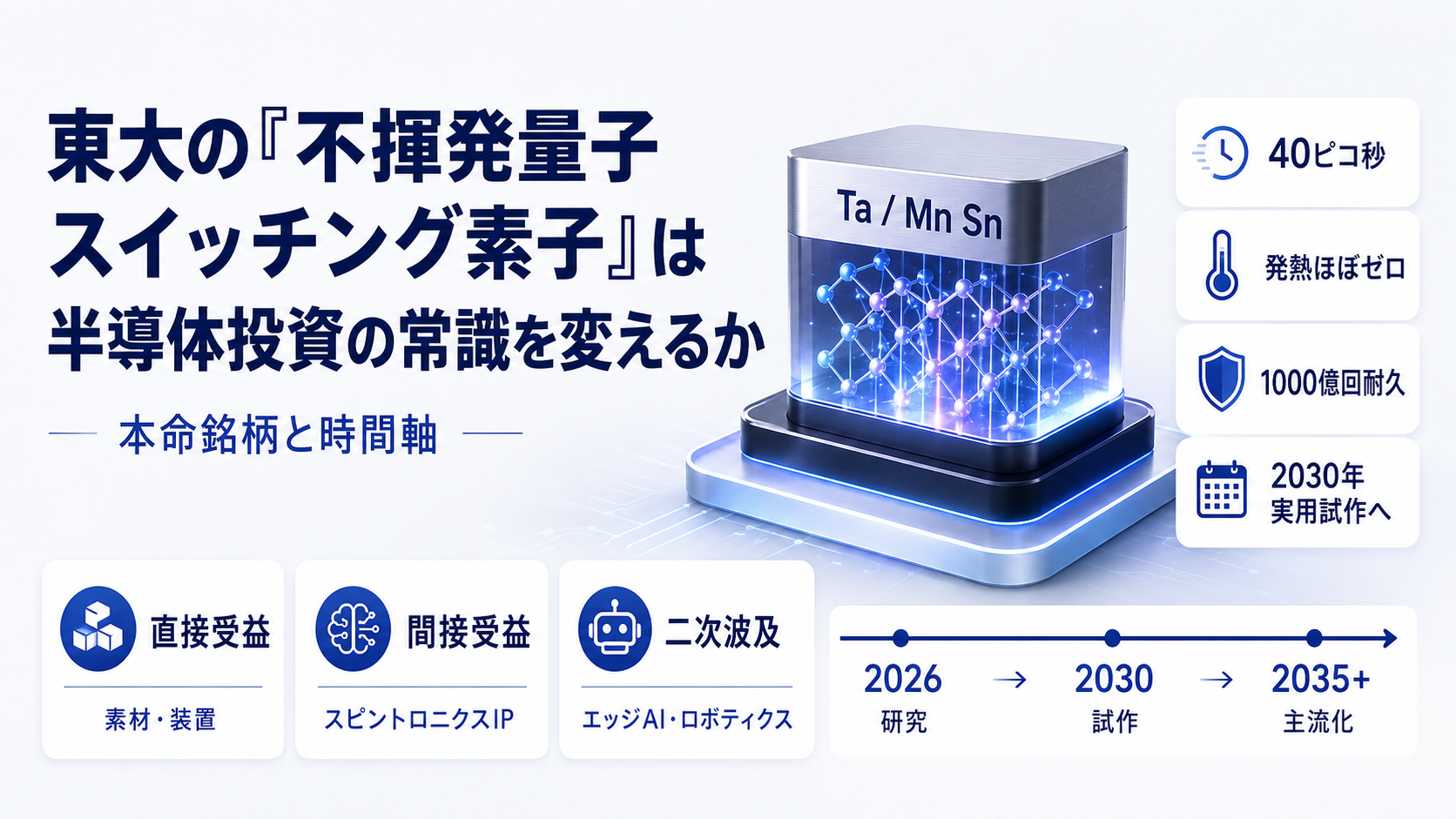
1000× faster, drastically less heat, 100 billion endurance cycles — UTokyo's May 2026 Science-published spin device targets a 2030 commercial trial. A CVC sorts material, equipment, and IP-holding tickers and maps second-order ripple effects into edge AI / robotics across time horizons.


Will the University of Tokyo's Nonvolatile Quantum Switching Element Rewrite Semiconductor Investing? Key Names and the Timeline
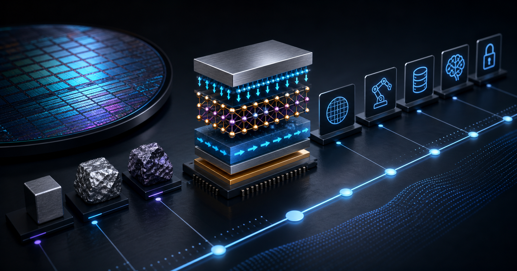
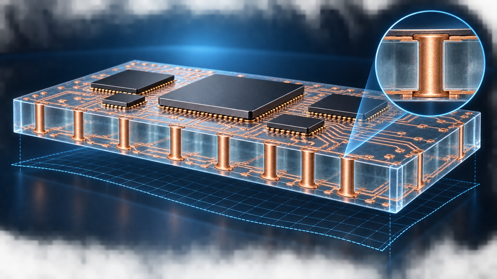
I started my career as an in-line process engineer building automotive EEPROM, slamming TCAD against memory device behavior hundreds of times. So when Nikkei reported on May 14, 2026 about the University of Tokyo team's "nonvolatile quantum switching element" — built from tantalum and manganese-tin, switching a bit in 40 picoseconds, and emitting almost no heat — two things hit me at once. First, "that's real physics." Second, "2030 prototype" is exactly the awkward distance for an investor. Below I break it down as an investment theme, cold-eyed. The investment-roadmap side — the equipment, materials, and IP that move before mass production — is covered in the companion post.
Reading "1000× Faster" the Way an Investor Should
Let me re-table the headline numbers from the investor's seat.
| Metric | Value | Comparison | Implication |
|---|---|---|---|
| Bit switching time | 40 picoseconds | ~1/1000 of conventional | Lifts the device-side ceiling on compute throughput |
| Mechanism | Spin (electron magnetization) flip | Different family from current-driven transistors | Sidesteps the dominant source of Joule heat |
| Endurance | Stable >100 billion cycles | Comparable to or beyond DRAM | Plausible for both volatile and nonvolatile roles |
| Materials | Tantalum + manganese-tin | No rare earths, existing fab materials | Supply-chain lock-in is relatively mild |
| Prototype target | 2030 | — | Mass production realistically late 2030s |
In my eyes, the bigger prize is on the heat side rather than the speed side. AI data-center TCO is increasingly rate-limited by cooling and power, not compute. A single Nvidia GB200 rack draws ~120 kW, and utility and HVAC capex can't keep up. A device-level cut in heat generation is exactly the kind of event that loosens an entire AI-infrastructure constraint by one notch.
Speed is a story about "how many chips you can run." Heat is a story about "how long you can keep running them." The latter is the larger investable market — that's my current read.
How Is This Different from STT/SOT-MRAM?
A fair reader will ask "another MRAM?" I want to handle that carefully.
| Approach | Switching mechanism | Switching speed | Endurance | Production status |
|---|---|---|---|---|
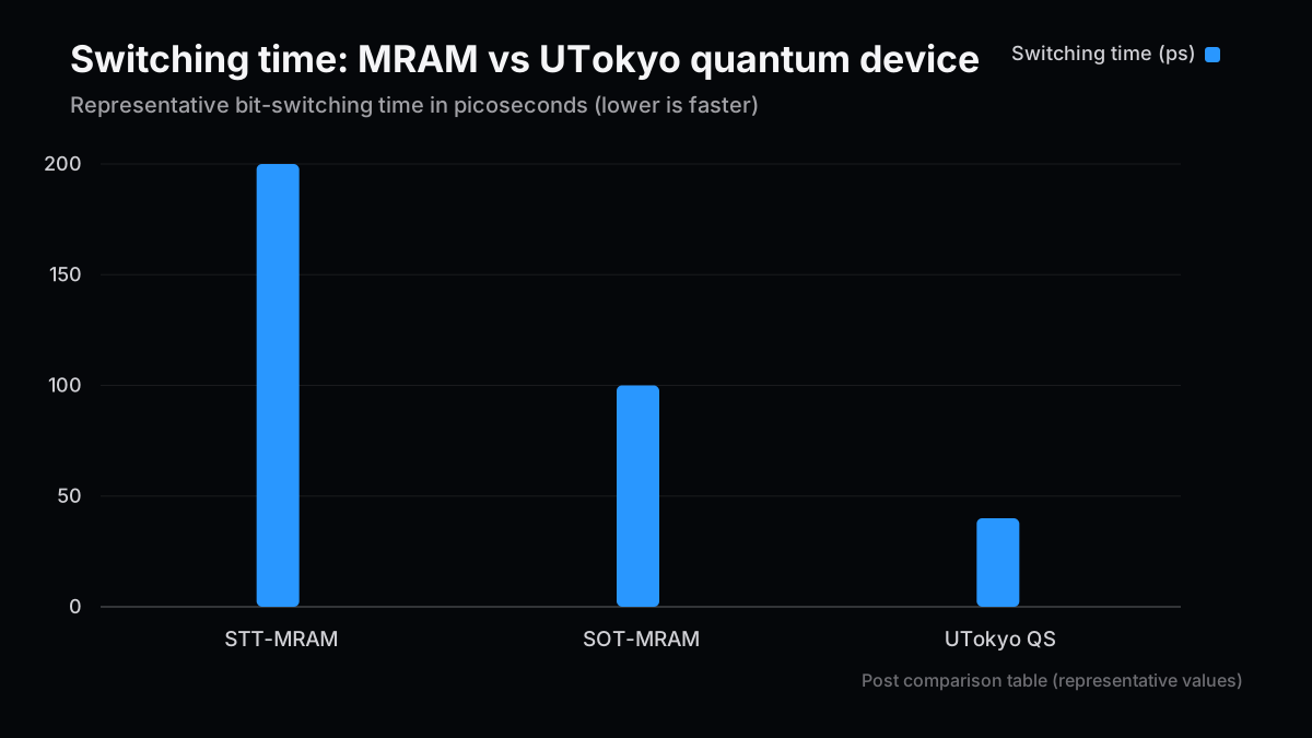
| STT-MRAM | Spin-transfer torque | ns to several hundred ps | ~10^12 cycles | Everspin, Samsung (partial eMRAM) in production |
| SOT-MRAM | Spin-orbit torque | ~100 ps | ~10^14 cycles | TSMC, Intel at research / pre-production |
| UTokyo nonvolatile quantum element | Quantum-state switching | 40 ps | >10^11 confirmed | Prototype, 2030 pre-mass-production target |
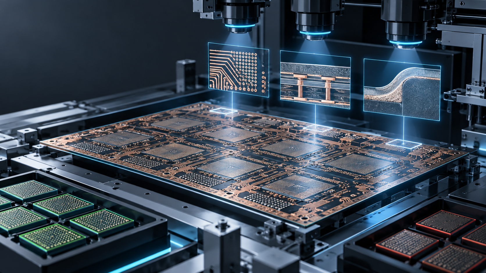
On paper this looks like "a faster SOT-MRAM." I don't want to over-simplify it. SOT-MRAM already has good CMOS process compatibility and sits at pre-production, while for the UTokyo element, the integration of a tantalum / manganese-tin stack with existing 300 mm lines is the gating risk going forward. In semiconductors, the gap between "physics works" and "yields above 90%" is always five to ten fab-years wide.
I lived this in EEPROM volume production: between a research "it switches" and a production "it switches at high yield, forever" there is a mountain of invisible inputs — CD control, particle management, tool-to-tool correlation. Every time a new-device headline lands, that mountain is the first thing I see.
Decomposing the Theme: Three Layers
When I write semi themes on ZYL0 I always split them into direct / indirect / second-order beneficiaries. Same frame here.
1. Direct: Materials and Equipment
| Category | Candidates | Logic |
|---|---|---|
| High-purity metals (Ta / Mn-based) | JX Metals (5016 JP), Sumitomo Chemical (4005 JP), Shin-Etsu Chemical (4063 JP) | Purity and film-uniformity become the bottleneck on the materials side |
| Deposition / sputter equipment | ULVAC (6728 JP), Tokyo Electron (8035 JP), Applied Materials (AMAT) | Spin devices live or die on stack uniformity; PVD/ALD differentiation surfaces |
| Metrology / inspection | KLA Corp (KLAC), Lasertec (6920 JP) | Inter-device variation inspection becomes one step harder |
| Power / EDA periphery | ROHM power semis, Cadence/Synopsys (EDA) | Designing low-heat devices into systems benefits the power/design side |
What's nice about this layer is that R&D spending creates demand even before any element reaches mass production. The 2026–2029 window is the pre-production prototype and capex phase, so equipment and materials see demand from R&D budgets first.
2. Indirect: Companies Sitting on Spintronics IP
| Name | Position | Comment |
|---|---|---|
| TDK (6762 JP) | Deep spintronics legacy from HDD magnetic heads | Patents and talent pool likely to monetize through licensing |
| Murata (6981 JP) | Spin-related IP via sensors and components | Asset-side, not P&L-side, leverage |
| Western Digital (WDC) | Sustained long-term spintronics R&D | US-side patents and licensing leverage |
This layer is priced on patent-pool and talent-scarcity premia rather than direct revenue. From a CVC seat, this is the kind of asset that surfaces in M&A and JV negotiations.
3. Second-Order: What Constraints Get Lifted, and Who Wins
This is the heart of the post. What is unlocked once device speed and heat improve by one to two orders of magnitude?
| Constraint relaxed | Application | Likely beneficiaries |
|---|---|---|
| Edge AI inference | Running larger models on phones, XR devices, industrial sensors | Apple (AAPL), Qualcomm (QCOM), Arm (ARM) |
| Physical AI / robotics | On-board inference under thermal/power budgets | Nvidia (NVDA), Boston Dynamics' parent, Fanuc (6954 JP), Yaskawa (6506 JP) |
| Satellites / spacecraft | Radiation tolerance × ultra-low power | Rocket Lab (RKLB), Mitsubishi Heavy Industries (7011 JP) space arm |
| Saturation of data-center cooling | Another step-up in per-rack compute density | Vertiv (VRT), Super Micro (SMCI), Eaton (ETN) |
Low-heat devices, in my view, create more value outside the data center than inside it. Inside the data center, heat can be absorbed by liquid and immersion cooling. Inside a phone or a robot, you physically cannot bolt on a cooling rig. The era of physical AI needs devices that allow AGI-class inference on a single battery, and most of that market lives outside the rack.
Timeline: Putting the 2026–2035 Roadmap on the Table
The most common error on new-device stories is the timeline. Here is my current view, framed for investors.
| Window | Stage | Investor action |
|---|---|---|
| 2026–2028 | Basic research, replication, patent jockeying | Thin, broad exposure to equipment/materials. Single-device bets are premature. |
| 2028–2030 | Pre-production prototyping, hyperscaler R&D entry | Track Intel/Samsung/TSMC R&D disclosures quarterly. Look for equipment orders. |
| 2030–2033 | Late-stage R&D, pilot production | Spin IP holders start moving on M&A / licensing. Add positions in those names. |
| 2033–2035 | Limited mass production, specialty integration | Second-order plays (physical AI, edge AI, space) start producing revenue |
| 2035– | Mainstream scenario (if production sticks) | Structural disruption to the NAND/DRAM cycle; Intel/Micron/Samsung capex mix shifts |
My personal rule of thumb: "Science-published, university-led, mass production in five years" elements actually reach mass production roughly 20–30% of the time. Right physics still has to clear the triple wall of tooling, yield, and cost. So for now, picking the surrounding demand around active device R&D pays off better — on a payoff × probability basis — than picking the device itself.
Scenario Analysis and Pitfalls
To close, I'll write the way I would for an investment committee — three scenarios.
| Scenario | Storyline | Subjective probability | Main beneficiaries |
|---|---|---|---|
| Base | Prototype chip in 2030, limited production in 2033, niche edge/space adoption | 50% | Equipment & materials, IP holders such as TDK, Apple/Qualcomm |
| Bull | Mainstream logic/memory integration by 2032, large-scale Intel/Samsung adoption | 20% | Intel, Samsung, Micron, Tokyo Electron, Applied Materials |
| Bear | Process compatibility never lands; SOT-MRAM and rivals eat the niche | 30% | Mass-production winners in existing spintronics (TSMC, Everspin) |
Three pitfalls. (1) Scaling limits — a single device that works in the lab is a different problem from a nanoscale array that switches in unison. (2) Process compatibility — whether a Ta / Mn-Sn stack avoids being treated as contamination in a standard CMOS line depends heavily on the toolmakers. (3) Incumbent response — Intel, Samsung, IBM have been running their own spin devices for years; this is "UTokyo printed a strong result," not "UTokyo invented spintronics."
If I were writing the IC memo, my guidance would be: avoid betting the device itself; take the theme through equipment, materials, and IP holders; re-evaluate startups in 2028–2030 at pre-production. It is the same playbook I used in semi-solid batteries — physics can be right and IRR can still die if you go in too early before mass production.
Reika1021's note.com post titled "Will the UTokyo new element break the semiconductor canon?" captures the mood well. My answer is: yes, the canon will change — but the change lands in the late 2030s. For now, take the periphery that benefits from active research, cleanly.
Next Issue Ideas
- Idea 1: A data-updated follow-up — Revisit the thesis with fresh numbers and separate what strengthened from what broke.
- Idea 2: A practical template edition — Turn the article into a checklist readers can reuse for investing, pricing, or technical operations.
- Idea 3: The bear-case test — Define the conditions that would invalidate this view and map the indicators to watch next.
Related Posts
- Spintronics Investment Roadmap 2030: Equipment, Materials, and IP Before the UTokyo Device — The practical sequel: how equipment, materials, inspection, and IP reprice before mass production
- Wait, We Don't Actually Know How the Universe Ends? JWST and DESI Are Cracking Cosmology — 3 Wild Theories Explained — Another frontier where new observations are shaking settled science, in plain language
References
The factual and numerical assumptions in this article are anchored to primary or public materials that readers can revisit during AdSense review and future updates.
This article is for informational purposes only and does not constitute investment advice or a recommendation of any specific stock, service, or contract structure. The author may hold positions or interests related to companies or services mentioned. Generative AI was used for parts of research, translation, and proofreading, with final review by ZYL0. See the disclaimer for details.