メモリとアクセラレータの距離を縮める実装基板技術:Elephantech・Absolics・Eliyanに見る次の開発方向性
Elephantechは基板製造のどこを変えるのか。 半導体パッケージ基板向けのDS-SAPは、表面とビア内の銅シード層を別々に形成し、微細配線とビア被覆の両立を狙う工程だ。2026年6月18日の公式発表は顧客との評価開始を示すが、量産歩留まりや量産採用数は示していない。開発・評価と量産を分けて読む必要がある。
P-Flexから発展した量産FPC、HDIビア向けDeepVia、パッケージ基板向けDS-SAPの違いは、Elephantechの銅配線技術を工程別に比較した続編で、銅使用量の再現計算とともに整理した。
ガラスコアの検索意図に対する短い答えは、低反りという材料特性だけでは量産性を判断できない、である。TGV、反り、panel yieldを同じ証拠段階で比較した続編では、Intel、NIST、Samsung Electro-Mechanics、Corningの一次資料と再現計算から、試作・pilot・量産を分けた。
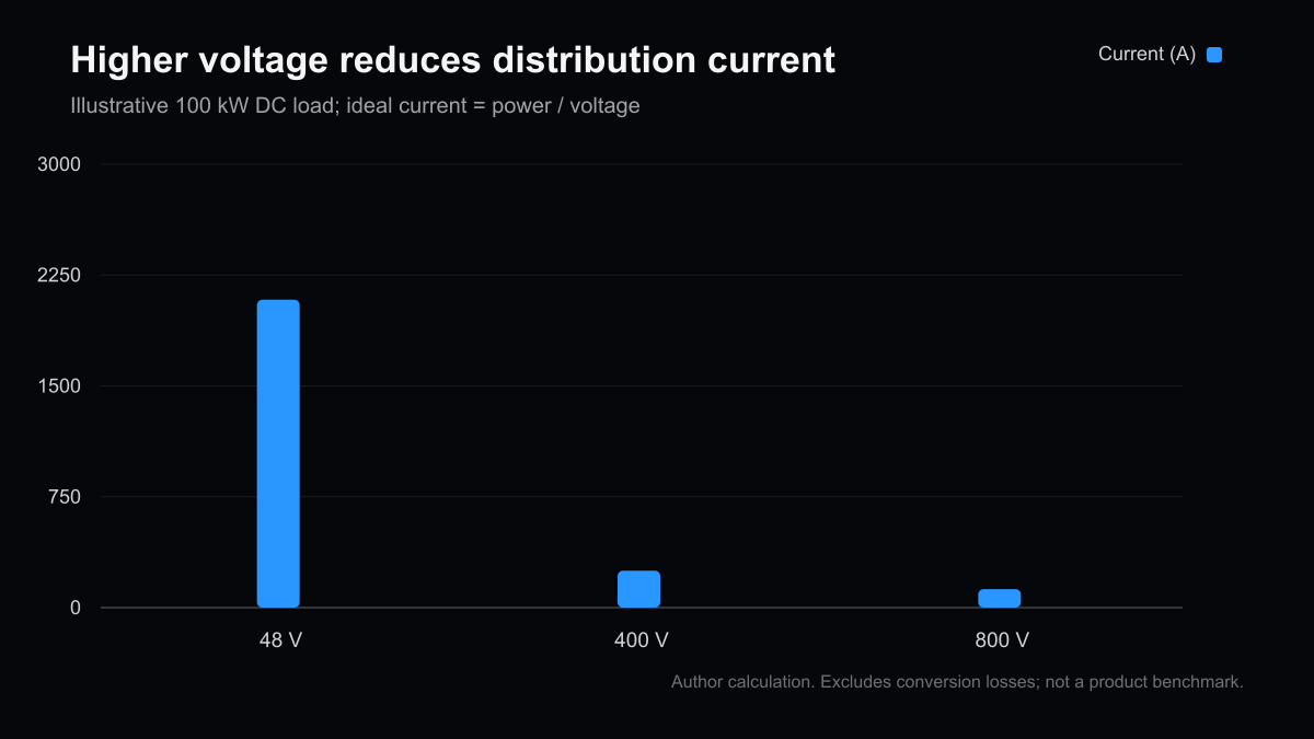
信号を運ぶ基板の課題に加え、ラックへ電力を届ける側を調べるなら、800V配電とGaN・SiCの役割、電流・効率の比較を参照してほしい。
2026年9月17日追記:冒頭の回答とDS-SAPの工程表現を公式資料で確認し、Elephantechおよびガラスコア量産課題の関連記事へ接続した。その他の企業情報は下記の当初確認日時点。今回の更新は自動処理で、人によるレビュー済みとはしていない。
自動車向けEEPROMのプロセス開発をしていた頃、量産直前になって基板の反り(warpage)がリフロー工程で暴れて歩留まりを崩す、という事態に何度も遭遇した。原因を追うと、たいていはダイとパッケージ材料の熱膨張係数(CTE)のわずかな差に行き着く。ANSYSやAutodesk Fusion 360で構造シミュレーションを回し、温度サイクルでどこに応力が集中するかを可視化してから金型と積層構成を直す——というのが当時の私の日課だった。今回、AbsolicsのガラスコアAI基板やElephantechの半導体パッケージ基板向け新工法のニュースを追っていて、「これは規模とお金の桁が違うだけで、あの頃と同じ喧嘩だ」と感じた。
前回はd-MatrixやTetraMemを軸に、チップの中でメモリと演算器の距離をどう詰めるかを書いた。今回はその一つ外側、チップとチップの間、つまり実装基板・パッケージ・ボードのレイヤーに焦点を移す。d-MatrixやTetraMemがダイの中の壁を攻めているとすれば、本稿で扱う会社群はダイの外の壁——パッケージ基板、プリント基板、そしてラック配線——を攻めている。同じ「メモリの壁」でも、戦場が違えば求められる性能指標も、勝ち筋も変わってくる。
バージョン注記: 企業の製品・調達・出荷状況は2026年8月17日時点で、各社公式発表と業界専門メディアの報道を中心に確認しています。性能値・投資額は各社の公表資料や報道ベースであり、将来の成果や横並び比較を保証するものではありません。
| テーマ | 学べること |
|---|
| 距離の階層構造 | ダイ間(1mm未満)からラックスケール(数m)まで、「距離」は4つの層に分解できる |
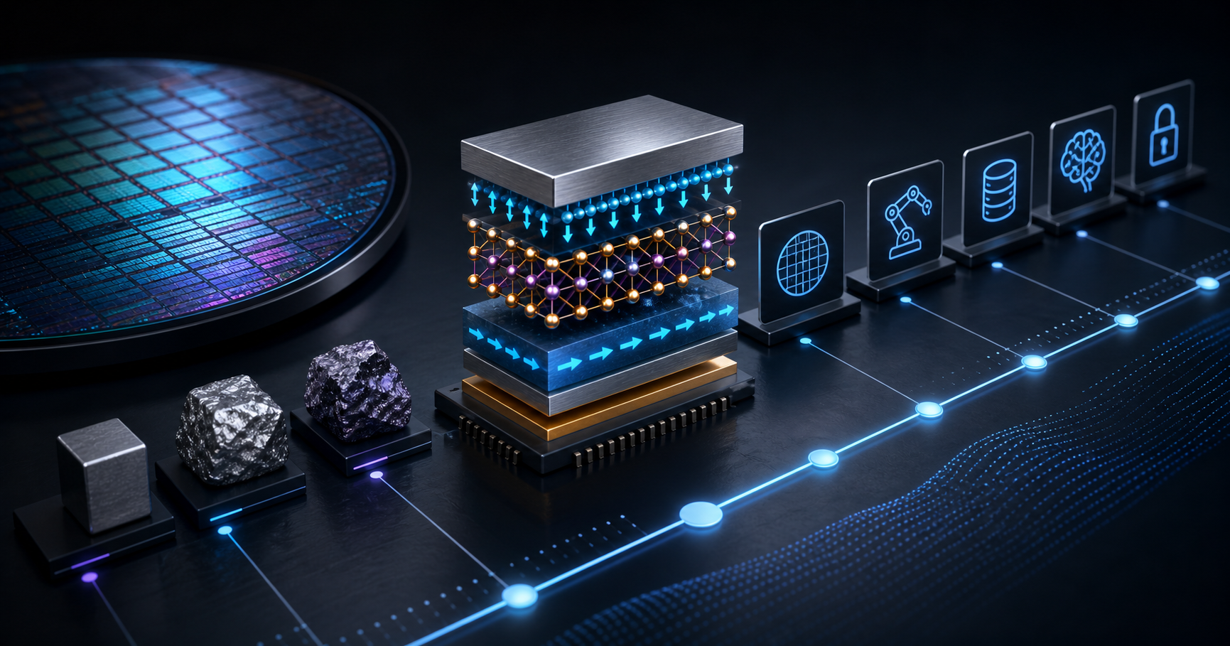
| 基板そのものを作り替える | Elephantechの添加法配線とAbsolicsのガラスコア基板は、同じ課題に別の材料・製法で挑んでいる |
| 接続を賢くして距離を消す | Eliyanのダイ間PHYは、インターポーザーなしで同等の帯域・電力効率を狙う |
| 距離を諦めて光に逃がす | Ayar Labsの共同パッケージ光学(CPO)は、ラックスケールの距離を電気配線ではなく光で解決する |
| 資金の勢い | 2026年だけでもElephantech・Absolics・Ayar Labsに数百億円〜数百億ドル規模の資金が動いている |
結論から言うと、「メモリの壁」は単一の壁ではなく、距離ごとに性質の違う4つの壁が積み重なったものだと私は考えている。
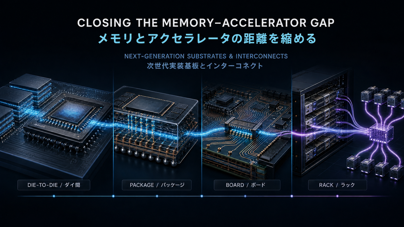
AIアクセラレータが重みを読み書きするとき、信号はダイの中だけでなく、ダイの外、パッケージの中、基板の上、そして場合によってはラックの中のケーブルまで移動する。それぞれの区間で、静電容量、抵抗、そして電力コストの性質が変わる。ダイ間(2.5Dインターポーザーやハイブリッドボンディング)であれば距離は1mm未満、パッケージ基板であれば数十mm、プリント基板上のチップ間であればセンチメートル単位、ラック内配線であればメートル単位まで広がる。距離が10倍になるごとに、配線に使う材料も、必要な設計思想も別物になる。
私がこの記事で言いたいのは単純なことで、「メモリとアクセラレータの距離を縮める」という一見わかりやすいスローガンの中に、実は「どの層の距離を、どういう方法で縮めるのか」という4つの異なる問いが隠れているということだ。ある会社は物理的に基板そのものを薄く精緻にすることで距離を削り、別の会社はインターポーザーという中間層を省略することで距離を消し、また別の会社は距離を縮める代わりに光という別の物理現象に逃げ込む。
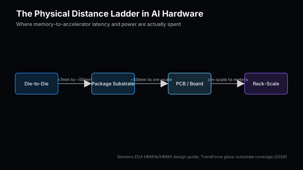
この4層を整理すると、次のようになる。
| 層 | 代表的な距離 | 主な技術 | 代表的なプレイヤー |
|---|
| ダイ間 | 1mm未満 | 2.5Dシリコンインターポーザー、ハイブリッドボンディング | TSMC CoWoS、Eliyan NuLink |
| パッケージ基板 | 数十mm | 有機ABF基板、ガラスコア基板、添加法配線 | Absolics、Elephantech |
| プリント基板/ボード | センチメートル単位 | 多層PCB、微細配線 | Elephantech(汎用多層PCB) |
| ラックスケール | メートル単位 | CXLファブリック、共同パッケージ光学(CPO) | Panmnesia、Ayar Labs |
実装前に距離とエネルギーコストの関係を大まかに掴んでおくと、どの層の問題なのかを見誤りにくい。厳密な信号解析の代わりに、私は次のような荒いモデルを最初の「会話のたたき台」として使っている。
# Rough mapping from physical distance to interconnect tier
# (order-of-magnitude only; real design points vary by generation)
TIERS = [
    (1.0, "die-to-die (2.5D interposer / hybrid bonding)"),
    (50.0, "package substrate (organic ABF / glass core)"),
    (500.0, "board-level (multilayer PCB, additive fine-pitch)"),
    (float("inf"), "rack-scale (CXL fabric or co-packaged optics)"),
]


def interconnect_tier(distance_mm: float) -> str:
    for limit, label in TIERS:
        if distance_mm <= limit:
            return label
    raise ValueError("unreachable")


def relative_energy_cost(distance_mm: float, pj_per_bit_per_mm: float = 0.15) -> float:
    # Energy roughly tracks trace length once a channel is electrically long;
    # this is a first-pass gut check, not a signed-off SI budget.
    return distance_mm * pj_per_bit_per_mm
このコードは実際のSI(信号品質)設計を代替するものではない。ただ、ある技術のニュースを読んだときに「これはダイ間の話か、基板の話か、それともラックの話か」を一瞬で仕分けるためのフィルタとしては十分に機能する。HBM4の世界で言えば、JEDECが2025年4月に標準化したHBM4は2048ビット幅・32独立チャネル構成で、スタックあたり2.0TB/s超(高度な構成では3.3TB/s)を実現し、2026年前半から量産が本格化した。CoWoSのような2.5D構成では、シリコンインターポーザーがサブ2μmの線幅・間隔でHBMとプロセッサをわずか数ミリの距離で結ぶ——DDRモジュールがプリント基板上を数十センチメートル引き回されるのとは、まったく違う世界線だ。
この節の主役は、配線という古典的な問題を、まったく違う角度から殴りにいっている2社だ。
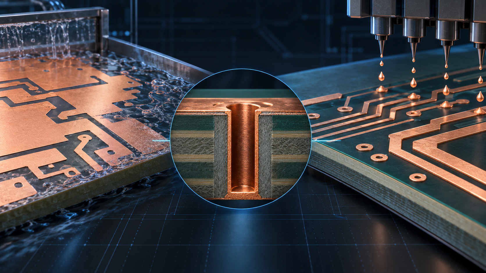
東京のElephantechは、SustainaCircuitsという独自の添加法(アディティブ)配線技術で知られるスタートアップだ。従来のプリント基板製造は、銅箔を貼った基材を薬液でエッチングして不要な部分を溶かす「サブトラクティブ(減算)法」が主流で、使う銅の大半が廃液として捨てられる。SustainaCircuitsは逆に、インクジェットで銅ナノ粒子インクを必要な場所にだけ「刷って」回路を形成する。同社の発表によれば、この方式は従来法に比べて銅使用量を70%、CO2排出量を75%削減できるという。
2026年3月12日、Elephantechは三菱電機から40億円のシリーズFを調達したと発表した。狙いは明快で、SustainaCircuits用インクジェット装置の量産能力を強化し、世界の基板メーカーへの導入を加速すること。プリント基板の世界市場は約10兆円規模とされ、三菱電機の産業機器としての量産・保守ノウハウとElephantechのナノ材料・インクジェット技術を組み合わせて、汎用多層PCBという大きなパイの一部を取りにいく構図だ。
私がこの記事のために調べていて一番驚いたのは、2026年6月18日に発表されたDS-SAP(Dual-Seed Semi Additive Process)だった。これは半導体パッケージ基板向けに特化した新工法で、従来のセミアディティブ法が抱えていた「表面には薄いシード層が欲しいが、アスペクト比の高いビア(貫通穴)には十分な厚みのシード被覆が欲しい」という、二律背反のトレードオフを解決しようとしている。DS-SAPは、無電解銅めっきまたはPVDで表面にごく薄いシード層を先に作り、その後にビアへ銅ナノ粒子インクを塗布して不足するシード層を補完する二段階構成にすることで、微細な表面配線と信頼性の高いビア被覆を両立させる。25μm径のビアでの実証データも公開されており、複数のAI半導体メーカーとアドバンストパッケージング企業が評価を始めているという。
一方、SK subsidiaryのAbsolics(Applied Materialsが約30%の株式を保有)は、まったく違う切り口を選んだ。有機ABF基板の代わりに、ガラスをコア材料に使う「inProut」プラットフォームだ。
ここで私のEEPROM時代の経験が生きてくる。有機基板は温度によって伸び縮みする量(CTE)がシリコンダイと大きく異なり、パッケージが大きくなるほど反りが無視できなくなる。私がリフロー工程で追いかけていたのは、まさにこの「基材とダイの膨張のズレが、どこにどれだけの応力を生むか」という問題だった。ガラスはシリコンに近いCTEを持ち、しかも円形のシリコンウェハーと違って四角いパネルで大面積に加工できるため、理論上は反りを抑えたまま基板を大きく・薄く・微細にできる。「なぜわざわざガラスなのか」と最初は思ったが、CTEミスマッチという物理を知っていると、この選択は驚くほど筋が通っている。
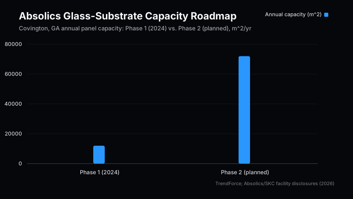
Absolicsは米国CHIPS法から製造向けに7500万ドル(2024年5月)、研究開発向けに1億ドル(2024年12月)の支援を受け、ジョージア州コビントンの工場を整備してきた。報道によれば同工場への投資額は6億ドル規模とされる。2026年1月時点で、AMDのMI400世代向けに量産グレードのサンプル出荷を開始し、Amazonへの供給も進んでいると報じられている。さらに年間パネル生産能力を1.2万平方メートルから7.2万平方メートルへと6倍に引き上げる「フェーズ2」拡張が進行中だ。
もっとも、ガラス基板はまだ「割れやすく、コストが高い」という現実的な弱点を抱えている。業界の見立てでは、2026年は2万ドルを超える最上位AIアクセラレータ向けの「ハイエンド採用元年」であり、ワークステーションやゲーミング向けまで裾野が広がるのは2028年頃と見られている。ElephantechとAbsolicsは、狙っているレイヤー(汎用多層PCB寄りかパッケージ基板寄りか)も、賭けている基材(銅の刷り方かガラスという素材そのものか)も違うが、どちらも「基板という受動的な脇役を、能動的な設計対象に変える」という同じ方向を向いている。
| 項目 | Elephantech(SustainaCircuits / DS-SAP) | Absolics(inProut ガラスコア) | 従来型有機基板(ABF) |
|---|
| 基材 | 樹脂基材+添加法銅配線 | ガラスコア | 有機樹脂(ABFフィルム) |
| 製法 | インクジェット銅ナノ粒子印刷+めっき/PVD | ガラスパネル加工+微細ビア形成 | サブトラクティブ・セミアディティブ |
| 得意なレイヤー | 汎用多層PCB、半導体パッケージ基板の微細配線 | 大型AIアクセラレータのパッケージ基板 | 汎用パッケージ基板全般 |
| 強み | 銅使用量70%減・CO2排出75%減、微細ビア被覆の両立 | 低反り・大面積パネル・微細配線密度 | 実績豊富、コスト・供給網が成熟 |
| 課題 | 量産ラインへの本格導入はこれから | 割れやすさ・コスト、量産歩留まりの立ち上げ | 大型化するほど反りが支配的に |
| 2026年時点の状況 | AI半導体メーカーとの評価開始(DS-SAP) | AMD MI400向け量産サンプル出荷開始 | 主流として稼働中 |
基板そのものを作り替えるのではなく、「賢い配線設計で高価なインターポーザーを丸ごと省略する」という第三の道を選んだのがEliyanだ。
Eliyanが開発するNuLink PHYは、UCIe(Universal Chiplet Interconnect Express)とBoW(Bunch of Wires)という2つの業界標準に対応するダイ間接続IPで、40〜130マイクロメートルという幅広いバンプピッチで動作する。TSMCの3nmプロセスでテストチップを作った後、Samsung FoundryのSF4X(4nm)にも展開した最新世代のNuLink-2.0は、1バンプあたり64Gbpsを達成しており、これはダイ間PHYとして業界最高水準だとEliyanは主張している。狙っているのはまさにHBM4クラスのメモリデバイスだ。
ここで私は一度、素朴な疑問にぶつかった。本当にインターポーザーを丸ごと不要にできるのか——それは話がうますぎないか、と。だが仕様を読み込むと、主張はもう少し的が絞られていた。NuLink-SP(Standard Packaging)というバリアントは、標準的な有機基板の上で、1パッケージあたりのHBM搭載数を最大4倍に増やせるとしている。しかもインターポーザーの量産準備を待つ必要がなくなることで、パッケージング・テスト・組み立てのコストを2倍以上削減し、量産までのリードタイムを最大26週間短縮できるという。つまり「インターポーザー並みの帯域・電力効率を、インターポーザーなしの標準パッケージで達成する」というのが正確な主張であり、あらゆる用途でインターポーザーが不要になるという話ではない。それでも、この主張が成り立つ範囲では、パッケージ基板の層そのものをスキップできることになる。
| 項目 | NuLink-2.0(先端バンプピッチ) | NuLink-SP(標準パッケージ向け) |
|---|
| 対応バンプピッチ | 40〜130μm | 標準有機基板の実装公差に対応 |
| 1バンプあたり帯域 | 64Gbps(3nmプロセス) | インターポーザー相当の帯域・電力効率を狙う |
| HBM搭載数への影響 | - | 同一パッケージでHBM搭載数を最大4倍に |
| コスト・リードタイム影響 | - | パッケージング/テストコストを2倍以上削減、リードタイムを最大26週間短縮 |
この動きは、HBM4という規格そのものの読み方にも影響する。JEDECが定めたHBM4は物理的な信号仕様であり、その信号をインターポーザー経由で運ぶかNuLinkのような標準パッケージ向けPHY経由で運ぶかは、規格の外側の設計判断だ。距離を縮める競争の一部は、こうして「基板の物理」から「配線IPの賢さ」へと重心を移しつつある。
ここまでの3社は、いずれもミリメートル単位の距離を削る戦いをしていた。だがラックスケール、つまりメートル単位の距離になると、話はまったく別の物理に切り替わる。
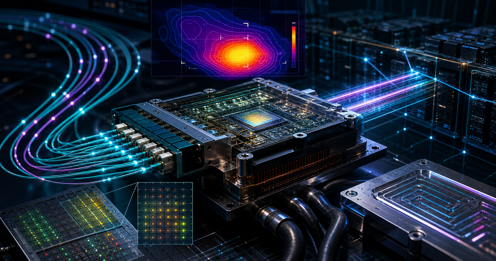
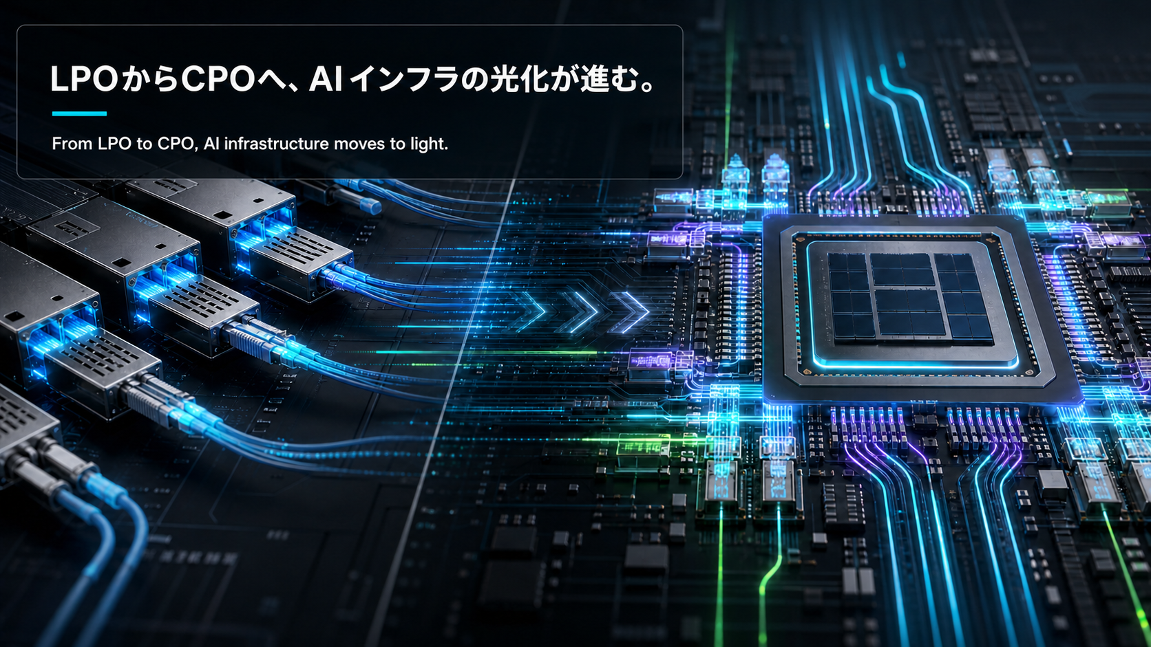
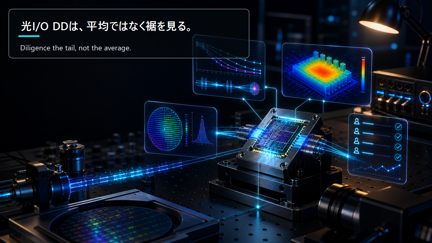
銅配線の減衰は距離とともに指数関数的に悪化するため、メートル単位の距離を電気信号だけで賄おうとすると、リピーターや複雑な等化回路が必要になり、消費電力が跳ね上がる。Ayar Labsが手がける共同パッケージ光学(CPO: Co-Packaged Optics)は、この区間を電気ではなく光で運ぶことで、そもそも「距離による劣化」という土俵から降りてしまう発想だ。これは過去に光I/OスタートアップのDDフレームを整理した回や、CPO量産の歩留まり・熱設計を扱った回で書いた論点の延長線上にある。
Ayar Labsは2026年3月3日、Neuberger Berman主導で5億ドルのシリーズEを完了したと発表した。これで累計調達額は約8.7億ドル、評価額は37.5億ドルに達している。投資家リストにはARK Invest、Insight Partners、カタール投資庁(QIA)、Sequoia Global Equities、1789 Capitalに加え、AMD・Alchip・MediaTek・NVIDIAといった戦略投資家が名を連ねる。半導体の川上から川下までがこぞって出資しているという事実は、CPOが「面白い技術」の段階を超えて「サプライチェーンに組み込むべきインフラ」だと業界が判断していることの表れだと私は読んでいる。
2025年11月には、台湾のASICデザインハウスGUCと組み、光エンジンを先端パッケージング・ASICの設計フローに統合すると発表した。さらに2026年3月のOFCでは、ODMパートナーのWiwynnと共同で、1,024基を超えるGPUを1つのシステムとして束ねるラックスケールのリファレンス設計を発表している。全面液冷、HVDC電源、ELSFP SuperNovaという遠隔光源方式を組み合わせた構成だ。
私がここで面白いと思うのは、CPOがElephantechやAbsolicsとは「距離への態度」がまったく逆だという点だ。ElephantechとAbsolicsは基板を物理的に作り替えて距離そのものを縮めようとしている。Ayar Labsは距離を縮める努力を諦め、その代わりに光という距離による損失がほぼ無視できる媒体に逃げ込んでいる。どちらも最終的には「メモリとアクセラレータの間でデータを速く・安く動かす」という同じゴールに向かっているのに、採るアプローチは正反対だ。
最後に紹介するPanmnesiaは、ここまでの4社とはやや異質な問いを投げかけてくる会社だ。
韓国のファブレススタートアップPanmnesiaは、CXL(Compute Express Link)を軸にしたスイッチシリコンとIPを開発している。2024年11月に6000万ドル超のシリーズAを評価額約2.5億ドルで調達し、これまでに17の投資家から総額約1.02億ドルを調達済みだ。2025年にはチップレット・メニーコアアーキテクチャ・PIM(Processing-in-Memory)・CXLを組み合わせてAIデータセンターのアーキテクチャを刷新する3000万ドル規模の政府系プロジェクトに採択され、2026年初頭にはAIアクセラレータ同士を直接つなぐチップ間相互接続技術を対象とした1000万ドルの追加プロジェクトも獲得している。2026年4月にはPCIe 6.4対応のCXL 3.2融合スイッチのサンプルチップを発表した。
ここで私は自分の議論に一度、待ったをかけたくなった。CXLでメモリをプールし、複数のアクセラレータから共有できるようにすることは、本当に「距離の問題を解決した」と言えるのだろうか。それとも、距離という物理的な制約を、単にソフトウェア的な抽象化の向こう側に押しやっただけではないか——考えてみると、答えは両方とも部分的に正しい。CXLファブリックは電気的な意味での物理距離を1mmにはしない。だがメモリを「特定のアクセラレータの隣に固定する」という制約そのものを外し、必要な容量を必要な場所にプールして配る、という別の解決策を提示している。Eliyanが「インターポーザーという中間層を省く」ことで距離の問題を再定義したように、Panmnesiaは「同じダイやパッケージに乗せる必要があるのか」という、さらに一歩引いた問いを立てている。
私がAI半導体の技術シナジーマップを作るとき、企業を「距離を縮める側」と「距離を無効化する側」という軸で分けて見るようにしているのは、この経験があるからだ。ElephantechとAbsolicsは前者、Ayar LabsとPanmnesiaは後者、Eliyanはちょうど中間に位置する。同じ「メモリの壁」というスローガンを掲げていても、投資判断において問うべき論点はまったく異なる。
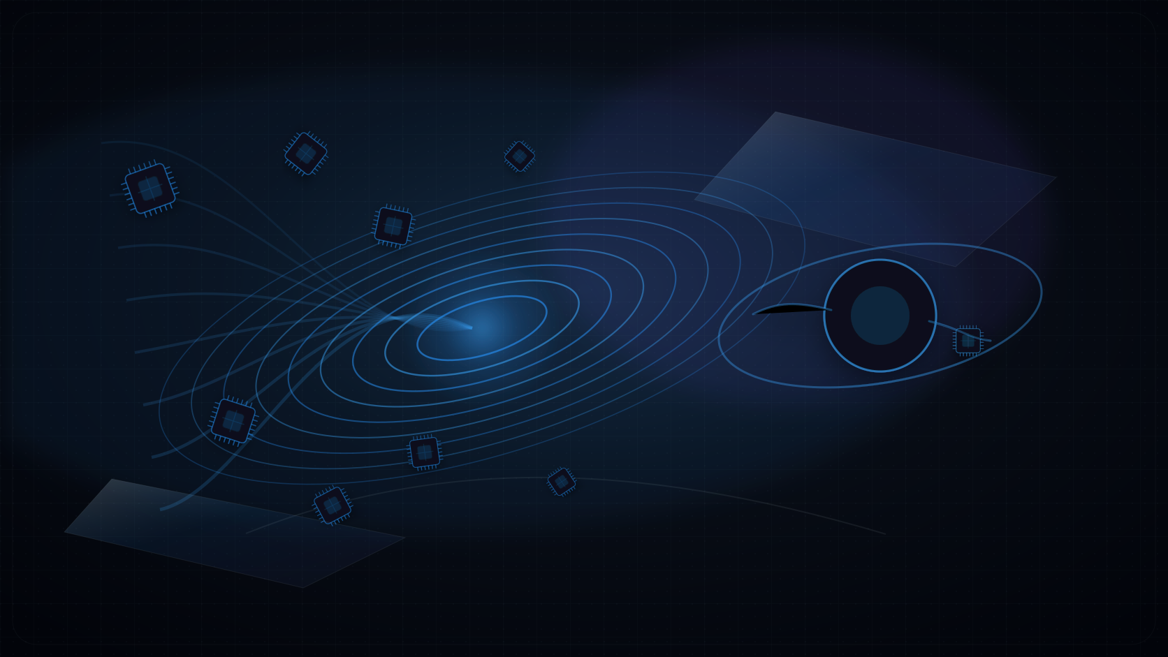
ここまでの5社を一枚の地図に落とすと、次の図になる。
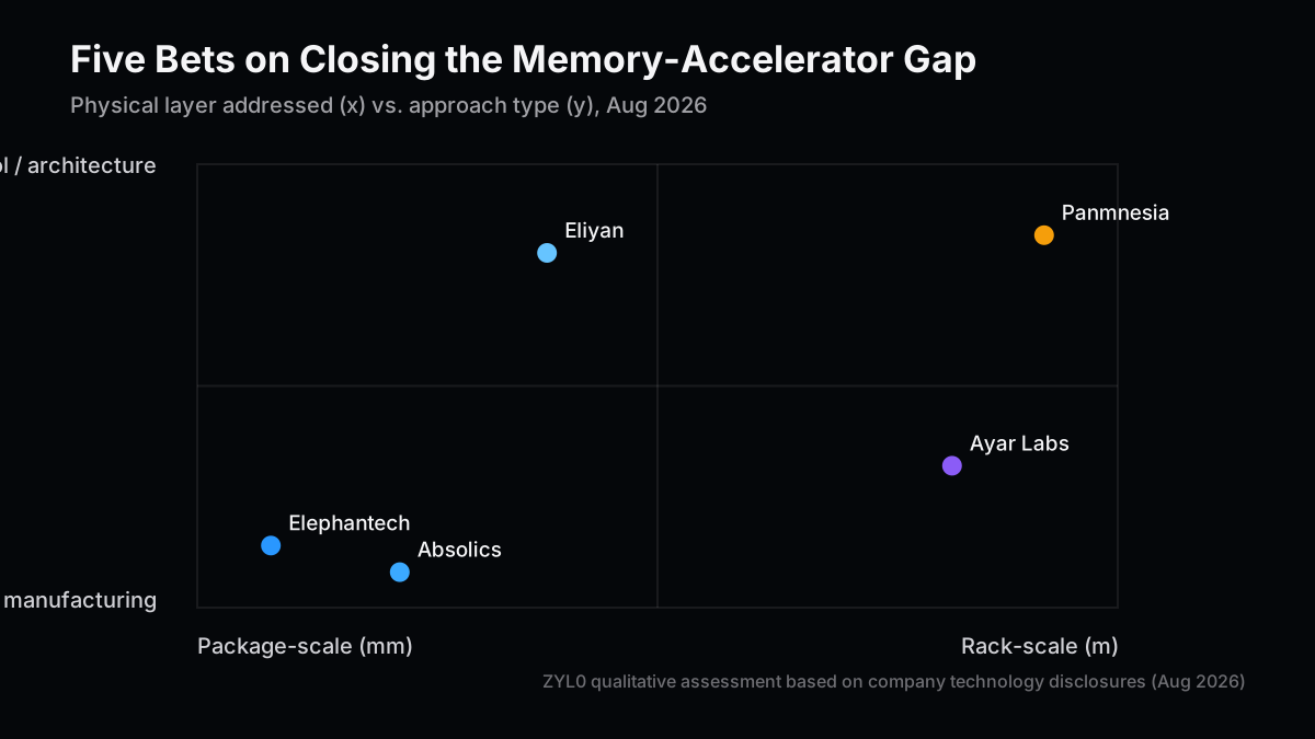
横軸がパッケージスケールかラックスケールか、縦軸が材料・製造の革新か、プロトコル・アーキテクチャの革新かを表している。ElephantechとAbsolicsは左下(パッケージスケール×材料革新)、Eliyanは左上寄り(パッケージスケール×プロトコル革新)、Ayar Labsは右下寄り(ラックスケール×物理媒体そのものの革新)、Panmnesiaは右上(ラックスケール×アーキテクチャ革新)に位置する。この4象限のどこにも、資金は同時に流れ込んでいる。
| 企業 | 直近の資金調達 | 評価額/規模の目安 |
|---|
| Elephantech | シリーズF 40億円(三菱電機、2026年3月) | 非公開 |
| Absolics | CHIPS法 計1.75億ドル(2024年)、コビントン工場約6億ドル | 非公開(SKC子会社) |
| Eliyan | 非公開(半導体メーカー各社への技術ライセンス中心) | 非公開 |
| Ayar Labs | シリーズE 5億ドル(2026年3月、累計8.7億ドル) | 評価額37.5億ドル |
| Panmnesia | シリーズA 6000万ドル超+政府系プロジェクト計4000万ドル | 評価額約2.5億ドル |
この地図から見えてくる今後の開発方向性は、私には3つある。
第一に、基板材料そのものの多様化が進む。ガラスコア、添加法配線、そして従来の有機ABFが、コストと性能のトレードオフに応じて棲み分ける方向に向かう。2026年時点でガラス基板が2万ドル超のAIアクセラレータ向けに限定されているように、すべてのワークロードが最先端基板を必要とするわけではない。
第二に、配線IPがパッケージング判断そのものを変える。Eliyanのような技術が実用段階に入るほど、「インターポーザーを使うかどうか」はコストと性能の連続的なトレードオフになり、設計者は距離を縮めるべきか、賢い接続で距離を無効化すべきかを、プロジェクトごとに選べるようになる。
第三に、距離の問題がパッケージからラック、そしてデータセンター全体のアーキテクチャへと外側に広がっていく。CPOとCXLファブリックは、メモリとアクセラレータの関係を「隣に固定する」ものから「必要に応じてプールし、光で結ぶ」ものへと再定義しつつある。
実装基板に求められる性能指標も、この3つの方向に応じて変化している。線幅・間隔(μm)、ビアのアスペクト比、パネル/ウェハーサイズの拡張性、反り(warpage)とCTE整合性、帯域密度(GB/s/mm²)、エネルギー効率(pJ/bit、あるいはGB/s/W)、そしてコスト・量産立ち上げまでの期間——これらすべてを同時に最適化できる万能な基板は存在しない。HBM3が到達したGB/s/Wという指標一つを取っても、141.2GB/s/Wという水準はGDDR5比で3倍のスループットを2割の電力で実現した結果であり、ここに至るまでには基板・パッケージ・インターコネクトの各層が同時に進化してきた。
基板・パッケージング分野の記事で私が最も警戒しているのは、異なる文脈の数字を同じ土俵で比較してしまうことだ。
- デモと量産は別の段階の25μmビア実証や、NuLinkの64Gbps/バンプは、いずれも特定条件下でのデモ・実測値であり、量産ラインでの歩留まりを保証するものではない。
- 「インターポーザー不要」は用途限定の主張のNuLink-SPが省略できるのは特定の帯域・容量レンジでのインターポーザーであり、あらゆるHBM構成を代替するわけではない。
- 報道ベースの投資額は確定額ではないのコビントン工場投資額のように、報道ベースの数字は文脈(補助金込みか、複数フェーズの合算か)によって振れる。
- ガラス基板はまだニッチ:2026年時点では2万ドル超のAIアクセラレータ向けに限定されており、コスト構造が変わらない限り主流にはならない。
- CPO・CXLは異なる距離帯の解 LabsのCPOはラックスケール、EliyanのNuLinkはパッケージスケールの問題であり、両者を同じ土俵で「どちらが優れているか」と比較するのは論点のすり替えになる。
- この記事の見方が向かないケース:コスト最優先で帯域要求が緩いエッジデバイスや、既存の有機基板で十分間に合う設計には、この記事で扱った先端基板・先端インターコネクトへの投資判断はそのまま当てはまらない。ボトルネックがメモリ帯域でないなら、基板を先端化しても得られるリターンは小さい。
ベンダーの発表資料に目立つ数字を見つけたら、私はまず「その数字が崩れる条件」を探すようにしている。基板・パッケージングの分野では、この態度がちょうどいいくらいだと思う。
書き終えてみて、冒頭のEEPROM時代の反り対策と、今回調べた5社の技術が、驚くほど同じ構造をしていることに改めて気づいた。あのときの私は、ダイとパッケージ材料のCTEのズレという物理を相手に、シミュレーションと実測を行き来しながら答えを探していた。Elephantech、Absolics、Eliyan、Ayar Labs、Panmnesiaも、規模とお金の桁は違えど、同じように「物理的な制約とどう折り合うか」を、それぞれ違う層で、違う武器で解いている。
メモリとアクセラレータの距離を縮めるという課題に、唯一の正解はない。基板材料を変える会社もあれば、配線IPで中間層を省く会社もあり、距離を諦めて光に逃げる会社も、距離という概念自体を無効化しようとする会社もある。投資家としても技術者としても、私たちが最初にすべき仕事は「これはどの層の、どの種類の距離の話か」を正しく仕分けることだと思う。それさえ間違えなければ、あとは実測値がすべてを語ってくれる。
次号の記事案
- 案1:HBM4量産の歩留まりを追う|TSV・ハイブリッドボンディングの実測データで検算する — JEDEC標準化から量産初期に入ったHBM4の歩留まり動向を、SK Hynix・Samsung・Micron各社の開示情報で横断比較する。
- 案2:ガラス基板のコスト構造を分解する|AbsolicsとIntelの量産曲線はいつ交差するか — 2026年の「ハイエンド限定」から2028年の裾野拡大に向けて、ガラス基板のコストカーブを追跡する。
- 案3:CXLメモリプーリングを実際に測る|レイテンシとTCOでPanmnesia型アーキテクチャの損益分岐点を探す — CXLファブリック経由のメモリアクセスが、ローカルHBMと比べてどこまでレイテンシ増を許容できるかを実装レベルで検証する。
本文の数値・事実関係は、読者が確認できる以下の一次情報・報道に基づいています(2026年8月17日時点)。
この記事は情報提供を目的としたものであり、特定の銘柄・企業・製品・サービスの購入や投資を推奨するものではありません。性能値・投資額・評価額は各社の公表資料または報道ベースの数値であり、異なる条件間での比較や将来の成果を保証するものではありません。記事の調査、翻訳、校正の一部には生成AIを利用しています。2026年9月13日の追記・修正は自動処理によるものです。詳細は免責事項をご覧ください。
Closing the Distance Between Memory and Accelerators: What Elephantech, Absolics, and Eliyan Reveal About the Next-Generation Substrate
What does Elephantech change in substrate manufacturing? For semiconductor package substrates, DS-SAP forms the copper seed layers on the surface and inside vias separately, targeting fine traces alongside reliable via coverage. The official June 18, 2026 announcement reports customer evaluations but provides neither production yield nor volume-adoption counts. Development, evaluation, and production should be assessed separately.
The distinction among production FPCs evolved from P-Flex, DeepVia for HDI vias, and DS-SAP for package substrates is developed in a process-by-process follow-up on Elephantech's copper interconnect technology, including a reproducible copper-material calculation.
The short answer to the glass-core search intent is that lower-warpage material properties do not establish manufacturability. A follow-up comparing TGV, warpage, and panel yield at matched evidence stages separates test vehicles, pilot lines, and volume production using primary Intel, NIST, Samsung Electro-Mechanics, and Corning material plus a reproducible scenario calculation.
For the complementary question of delivering power to the rack, see the 800V distribution, GaN and SiC roles, and current and efficiency comparison.
September 17, 2026 update: The opening answer and DS-SAP process wording were checked against official material, and contextual links were added to the Elephantech and glass-core manufacturing follow-ups. Other company information retains the original verification date below. This update was automated and is not represented as human-reviewed.
Back when I was developing automotive EEPROM process technology, I ran into the same failure mode over and over right before volume production: board warpage going haywire during reflow and dragging yield down with it. Trace the cause far enough and it almost always came back to a small mismatch in coefficient of thermal expansion (CTE) between the die and the package material. My routine at the time was to run structural simulations in ANSYS or Autodesk Fusion 360, map out where stress concentrated across a thermal cycle, and then fix the mold and the layer stack-up before it ever hit the line. Reading through the news on Absolics' glass-core AI substrate and Elephantech's new process for semiconductor package substrates for this piece, I kept thinking: this is the same fight, just several orders of magnitude bigger in scale and money.
Last time, I wrote about d-Matrix and TetraMem and how they close the distance between memory and compute inside a single die. This time I want to move one layer outward — to the space between chips: the implementation substrate, the package, and the board. If d-Matrix and TetraMem are attacking the wall inside the die, the companies in this piece are attacking the wall outside it — the package substrate, the printed circuit board, and the wiring inside a rack. It's the same "memory wall," but the battlefield changes, and so does what actually counts as a winning move.
Version note: Product, procurement, and shipment status is as of August 17, 2026, drawn primarily from company announcements and trade-press coverage. Performance figures and investment amounts are vendor-reported or press-reported and should not be read as guarantees of future results or as directly comparable across companies.
| Topic | What you'll learn |
|---|
| The distance hierarchy | "Distance" splits into four layers, from sub-1mm die-to-die connections to meter-scale rack fabrics |
| Rebuilding the substrate itself | Elephantech's additive copper printing and Absolics' glass-core substrate attack the same problem with different materials and processes |
| Making the connection smarter | Eliyan's die-to-die PHY aims to match interposer-class bandwidth and power without an interposer |
| Giving up on distance, using light | Ayar Labs' co-packaged optics (CPO) solves rack-scale distance with light instead of copper |
| Capital momentum | Elephantech, Absolics, and Ayar Labs alone have pulled in hundreds of millions to billions of dollars in 2026 |
My conclusion up front: the memory wall isn't one wall. It's four walls of different character, stacked by distance.
When an AI accelerator reads or writes weights, the signal doesn't just travel inside the die — it crosses the package, the board, and in some cases cables inside a rack. Each segment has different capacitance, resistance, and power-cost characteristics. Die-to-die connections (2.5D interposers, hybrid bonding) run under 1mm; package substrates run tens of millimeters; chip-to-chip traces on a printed circuit board run centimeters; rack-level wiring runs meters. Every order-of-magnitude jump in distance changes both the materials in play and the design philosophy needed to handle it.
My point in this piece is simple: the tidy slogan "close the distance between memory and accelerators" hides four genuinely different questions — which layer's distance, closed by which method. One company physically thins and refines the substrate itself to shrink distance. Another eliminates an entire intermediate layer — the interposer — to make distance disappear from the bill of materials. A third gives up on shrinking distance altogether and escapes into a different physical medium: light.
Laid out as four tiers, it looks like this.
| Tier | Representative distance | Primary technology | Representative players |
|---|
| Die-to-die | Under 1mm | 2.5D silicon interposer, hybrid bonding | TSMC CoWoS, Eliyan NuLink |
| Package substrate | Tens of mm | Organic ABF substrate, glass-core substrate, additive wiring | Absolics, Elephantech |
| PCB / board | Centimeter scale | Multilayer PCB, fine-pitch routing | Elephantech (general-purpose PCB) |
| Rack-scale | Meter scale | CXL fabric, co-packaged optics (CPO) | Panmnesia, Ayar Labs |
Before deployment, it helps to have a rough sense of how distance maps onto energy cost, so you don't misdiagnose which layer's problem you're actually looking at. Instead of a full signal-integrity analysis, I use a deliberately crude model like this as a first conversation starter.
# Rough mapping from physical distance to interconnect tier
# (order-of-magnitude only; real design points vary by generation)
TIERS = [
    (1.0, "die-to-die (2.5D interposer / hybrid bonding)"),
    (50.0, "package substrate (organic ABF / glass core)"),
    (500.0, "board-level (multilayer PCB, additive fine-pitch)"),
    (float("inf"), "rack-scale (CXL fabric or co-packaged optics)"),
]


def interconnect_tier(distance_mm: float) -> str:
    for limit, label in TIERS:
        if distance_mm <= limit:
            return label
    raise ValueError("unreachable")


def relative_energy_cost(distance_mm: float, pj_per_bit_per_mm: float = 0.15) -> float:
    # Energy roughly tracks trace length once a channel is electrically long;
    # this is a first-pass gut check, not a signed-off SI budget.
    return distance_mm * pj_per_bit_per_mm
This code doesn't substitute for real signal-integrity work. What it does do is instantly sort a piece of news into "this is a die-to-die story," "this is a substrate story," or "this is a rack story." In HBM4 terms: JEDEC standardized HBM4 in April 2025 with a 2048-bit interface across 32 independent channels, delivering over 2.0TB/s per stack (up to 3.3TB/s in advanced configurations), and volume production ramped through early 2026. In a CoWoS-style 2.5D configuration, the silicon interposer routes HBM-to-processor connections at sub-2-micron line/space, across a distance of just a few millimeters — a completely different world from a DDR module running tens of centimeters across a printed circuit board.
The two companies in this section are attacking a classic problem — routing copper — from angles that have almost nothing in common.
Tokyo-based Elephantech is known for SustainaCircuits, a proprietary additive wiring process. Conventional PCB manufacturing is dominated by a subtractive process: you laminate copper foil onto a base material, then etch away everything you don't need, discarding most of the copper as waste. SustainaCircuits inverts that. It inkjet-prints copper nanoparticle ink only where a circuit is actually needed. According to the company, this cuts copper consumption by 70% and CO2 emissions by 75% versus the conventional process.
On March 12, 2026, Elephantech announced a ¥4 billion (roughly $27M) Series F from Mitsubishi Electric. The stated purpose is straightforward: scale up mass-production capacity for the SustainaCircuits inkjet equipment and accelerate adoption among PCB manufacturers worldwide. The global PCB market is estimated at roughly ¥10 trillion, and the partnership pairs Mitsubishi Electric's industrial-equipment manufacturing and support know-how with Elephantech's nanomaterial and inkjet expertise to go after a slice of the general-purpose multilayer PCB segment.
What surprised me most while researching this piece was DS-SAP (Dual-Seed Semi Additive Process), announced June 18, 2026. It's a process built specifically for semiconductor package substrates, and it targets a real trade-off in conventional semi-additive processing: you want an ultra-thin seed layer on the surface for fine patterning, but you also want thick, reliable seed coverage inside high-aspect-ratio vias — and conventional processes struggle to give you both at once. DS-SAP splits seed-layer formation into two independent stages: an ultra-thin surface seed via electroless copper plating or PVD, followed by copper nanoparticle ink applied to the vias to complete insufficient seed-layer coverage. The company has published demonstration data on 25-micron-diameter vias, and says it has begun evaluations with several AI semiconductor manufacturers and advanced-packaging companies.
Absolics — an SKC subsidiary roughly 30%-owned by Applied Materials — took a completely different angle. Instead of an organic ABF substrate, its inProut platform uses glass as the core material.
This is where my EEPROM-era experience comes back into play directly. Organic substrates expand and contract at a different rate than a silicon die (a CTE mismatch), and the bigger the package gets, the more that mismatch shows up as warpage you can't ignore. What I spent a good chunk of my process-development years chasing during reflow was exactly this: how a CTE mismatch between die and substrate concentrates stress, and where. Glass has a CTE much closer to silicon's, and unlike a round silicon wafer, it can be processed as a large rectangular panel — so in principle, you can build a bigger, thinner, more finely routed substrate while keeping warpage under control. My first reaction to "why glass, of all things" was skepticism. Once you factor in CTE mismatch as a physical constraint rather than a footnote, though, the choice makes a surprising amount of sense.
Absolics has drawn $75M in manufacturing support (May 2024) and $100M in R&D support (December 2024) from the US CHIPS Act to build out its Covington, Georgia facility, reportedly a roughly $600M investment. As of January 2026, the company had begun shipping volume-production-grade samples for AMD's MI400-series accelerators, with supply to Amazon reportedly underway as well. A "Phase 2" expansion is in progress to grow annual panel capacity sixfold, from 12,000 to 72,000 square meters.
Glass substrates still carry real, practical downsides: they're more fragile and currently more expensive than the alternative. The industry consensus is that 2026 is the "high-end adoption" year, reserved for AI accelerators priced above $20,000, with broader adoption into workstation and gaming markets not expected until around 2028. Elephantech and Absolics are targeting different layers (general-purpose PCB versus AI-accelerator package substrate) and betting on different materials (how you print copper versus the substrate material itself) — but both are pointed at the same underlying shift: turning the substrate from a passive supporting actor into an actively engineered part of the system.
| Item | Elephantech (SustainaCircuits / DS-SAP) | Absolics (inProut glass core) | Conventional organic substrate (ABF) |
|---|
| Base material | Resin substrate + additive copper wiring | Glass core | Organic resin (ABF film) |
| Process | Inkjet copper nanoparticle printing + plating/PVD | Glass panel processing + fine via formation | Subtractive / semi-additive processing |
| Layer it targets | General-purpose multilayer PCB, fine wiring on semiconductor package substrates | Package substrates for large AI accelerators | Package substrates broadly |
| Strength | 70% less copper, 75% less CO2, fine + reliable via coverage together | Low warpage, large-format panels, fine wiring density | Proven track record, mature cost and supply chain |
| Challenge | Full production-line adoption is still ahead | Fragility and cost, ramping production yield | Warpage becomes dominant as packages scale up |
| Status as of 2026 | Evaluations underway with AI semiconductor makers (DS-SAP) | Volume samples shipping for AMD MI400-class | Running as the mainstream default |
Instead of rebuilding the substrate, Eliyan chose a third path: engineer the interconnect smart enough that you can skip the expensive interposer altogether.
Eliyan's NuLink PHY is a die-to-die interconnect IP that supports two industry standards — UCIe (Universal Chiplet Interconnect Express) and BoW (Bunch of Wires) — across a wide range of bump pitches from 40 to 130 microns. After an early test chip on TSMC's 3nm process, the latest generation, NuLink-2.0, taped out on Samsung Foundry's SF4X (4nm) and hits 64Gbps per bump — which Eliyan describes as the industry's highest die-to-die PHY performance. The explicit target is HBM4-class memory.
I ran into a simple doubt here: can you really eliminate the interposer entirely? That sounded almost too convenient. Reading the spec more closely, though, the claim turns out to be narrower and more defensible than the headline suggests. NuLink-SP (the Standard Packaging variant) lets a design fit up to 4x more HBM stacks into a single package while running on an ordinary organic substrate. Because it removes the dependency on interposer readiness, it cuts packaging, test, and assembly costs by at least 2x and shortens time-to-market by up to 26 weeks. The real claim, in other words, is "match interposer-class bandwidth and power efficiency on a standard package, without an interposer" — not "no design ever needs an interposer again." Within the range where that claim holds, though, an entire layer of the packaging stack simply disappears from the bill of materials.
| Item | NuLink-2.0 (advanced bump pitch) | NuLink-SP (standard packaging) |
|---|
| Supported bump pitch | 40-130 microns | Fits standard organic substrate assembly tolerances |
| Bandwidth per bump | 64Gbps (3nm process) | Targets interposer-class bandwidth/power efficiency |
| Effect on HBM capacity | - | Up to 4x more HBM stacks in the same package |
| Effect on cost / lead time | - | Packaging/test cost cut by 2x+, lead time shortened by up to 26 weeks |
This also changes how you should read the HBM4 standard itself. JEDEC's HBM4 spec defines the physical signal; whether that signal travels through a silicon interposer or through a NuLink-class PHY on a standard package is a design decision that sits outside the standard. Part of the race to close distance has quietly shifted from "physics of the substrate" to "cleverness of the interconnect IP."
The first three companies were all fighting over millimeters. At rack scale — meters — the physics changes entirely.
Copper attenuation gets exponentially worse with distance, so trying to cover meter-scale runs with electrical signaling alone forces you into repeaters and complex equalization, and power consumption climbs fast. Ayar Labs' co-packaged optics (CPO) carries that segment with light instead, which means it doesn't play the "loss scales with distance" game at all. This extends a line of argument I covered previously in a diligence framework for optical I/O startups and in a piece on CPO ramp yield and thermal design.
On March 3, 2026, Ayar Labs closed a $500 million Series E led by Neuberger Berman, bringing total funding to roughly $870 million at a $3.75 billion valuation. The investor list runs from ARK Invest, Insight Partners, the Qatar Investment Authority, Sequoia Global Equities, and 1789 Capital to strategic backers AMD, Alchip, MediaTek, and NVIDIA. Reading that list, I take the fact that both upstream and downstream players in semiconductors are all writing checks as a signal that the industry has stopped treating CPO as "an interesting technology" and started treating it as infrastructure that belongs in the supply chain.
In November 2025, Ayar Labs partnered with Taiwanese ASIC design house GUC to integrate its optical engines into advanced-packaging and ASIC design flows. At OFC in March 2026, it announced a rack-scale reference design with ODM partner Wiwynn that stitches together more than 1,024 GPUs into a single system — fully liquid-cooled, HVDC-powered, using ELSFP SuperNova remote light sources.
What I find most interesting here is that CPO takes the exact opposite stance on distance from Elephantech and Absolics. Elephantech and Absolics physically rebuild the substrate to shrink distance itself. Ayar Labs gives up on shrinking distance and escapes into a medium — light — where distance-driven loss is close to a non-issue. Both are ultimately chasing the same goal — move data between memory and accelerators faster and cheaper — but they've picked opposite strategies to get there.
The last company on this list, Panmnesia, poses a slightly different question than the other four.
South Korean fabless startup Panmnesia builds switch silicon and IP centered on CXL (Compute Express Link). It raised a Series A of over $60M at roughly a $250M valuation in November 2024, bringing total funding across three rounds and 17 investors to about $102M. In 2025, it was selected for a $30M government-backed project to redesign AI datacenter architecture around chiplets, manycore designs, processing-in-memory (PIM), and CXL. Early 2026 brought an additional $10M government R&D project targeting direct chip-to-chip interconnects between AI accelerators, and in April 2026 the company announced a PCIe 6.4-compatible CXL 3.2 Fusion Switch sample chip.
Here I want to push back on my own framing for a moment. Does pooling memory over CXL and sharing it across multiple accelerators actually "solve" the distance problem? Or does it just push a physical constraint behind a layer of software abstraction? Thinking it through, both answers are partly right. A CXL fabric doesn't make the electrical distance 1mm. But it removes the constraint that memory has to sit physically next to one specific accelerator in the first place, and replaces it with pooling and allocating capacity wherever it's actually needed. Just as Eliyan redefines the distance problem by removing an intermediate layer — the interposer — Panmnesia asks an even more upstream question: does this memory need to sit on the same die or package at all?
I sort companies along a "shrinking distance" versus "nullifying distance" axis when I build technology synergy maps for investment cases, and this is exactly why. Elephantech and Absolics sit on the shrinking-distance side; Ayar Labs and Panmnesia sit on the nullifying-distance side; Eliyan sits right in the middle. All five wave the same "memory wall" banner, but the questions worth asking as an investor differ completely depending on where a company actually sits.
Plot all five companies on a single map and this is what you get.
The x-axis runs from package scale to rack scale; the y-axis runs from material/manufacturing innovation to protocol/architecture innovation. Elephantech and Absolics sit in the lower-left (package scale x material innovation); Eliyan sits toward the upper-left (package scale x protocol innovation); Ayar Labs sits toward the lower-right (rack scale x innovation in the physical medium itself); Panmnesia sits in the upper-right (rack scale x architecture innovation). Capital is flowing into every quadrant of this map at once.
| Company | Recent funding | Valuation / scale indicator |
|---|
| Elephantech | Series F, ¥4B (Mitsubishi Electric, March 2026) | Undisclosed |
| Absolics | $175M combined CHIPS Act support (2024), ~$600M Covington facility | Undisclosed (SKC subsidiary) |
| Eliyan | Undisclosed (primarily technology licensing to semiconductor makers) | Undisclosed |
| Ayar Labs | Series E, $500M (March 2026, ~$870M total raised) | $3.75B valuation |
| Panmnesia | Series A $60M+ plus ~$40M in government-backed projects | ~$250M valuation |
Three directions for development follow from this map, as I read it.
First, substrate materials keep diversifying. Glass core, additive wiring, and conventional organic ABF will settle into different niches based on cost-versus-performance trade-offs, rather than one material winning outright. As of 2026, glass substrates are confined to AI accelerators priced above $20,000 — not every workload needs a frontier substrate.
Second, interconnect IP starts to reshape the packaging decision itself. As technology like Eliyan's matures, "should this design use an interposer" turns into a continuous cost-versus-performance trade-off rather than a binary default, and designers get to choose project by project whether to shrink distance physically or nullify it with a smarter connection.
Third, the distance problem keeps expanding outward — from the package to the rack, and from the rack to the data-center architecture as a whole. CPO and CXL fabrics are redefining the relationship between memory and accelerators, from "fixed next-door neighbor" to "pooled capacity, connected by light, allocated on demand."
The performance metrics that matter for implementation substrates shift accordingly: line/space (microns), via aspect ratio, panel/wafer scalability, warpage and CTE matching, bandwidth density (GB/s per mm²), energy efficiency (pJ/bit, or GB/s per watt), and cost and time-to-volume. No single substrate optimizes all of these at once. Even a single metric like HBM3's rated 141.2 GB/s/W — three times GDDR5's throughput at roughly a fifth of the power — is the product of substrate, package, and interconnect all advancing together, not any one layer working in isolation.
The single riskiest habit in a packaging-and-substrate article is comparing numbers from different contexts as if they belonged on the same scale.
- Demos are not production: DS-SAP's 25-micron via demonstration and NuLink's 64Gbps-per-bump figure are both measured results under specific conditions — neither guarantees production-line yield.
- "No interposer needed" is a scoped claim: What Eliyan's NuLink-SP eliminates is the interposer within a specific bandwidth and capacity range, not every HBM configuration.
- Press-reported investment figures aren't final: Numbers like Absolics' Covington facility investment shift depending on context — whether subsidies are included, whether multiple phases are combined.
- Glass substrates are still a niche: As of 2026 they're confined to AI accelerators above $20,000, and won't go mainstream until the cost structure changes.
- CPO and CXL solve different distance bands: Ayar Labs' CPO addresses rack scale; Eliyan's NuLink addresses package scale. Comparing them head-to-head as "which is better" misses the point.
- Where this framing does not fit: For cost-first edge devices with modest bandwidth needs, or designs that a conventional organic substrate already handles comfortably, the investment case for the frontier substrates and interconnects covered here doesn't transfer directly. If memory bandwidth isn't the actual bottleneck, pushing to a more advanced substrate buys little return.
When I spot an eye-catching number in a vendor's release, my first move is to look for the conditions under which it falls apart. In substrates and packaging, that level of skepticism is about the right dose.
Having written all this out, I keep coming back to how closely the warpage fight from my EEPROM years mirrors what these five companies are doing today. Back then, I was chasing a CTE mismatch between die and package material, bouncing between simulation and physical measurement to find an answer. Elephantech, Absolics, Eliyan, Ayar Labs, and Panmnesia are, at a wildly different scale of money and stakes, solving the same underlying problem — how to make peace with physical constraints — at different layers, with different tools.
There's no single correct answer to closing the distance between memory and accelerators. Some companies change the substrate material. Some remove an intermediate layer with smarter interconnect IP. Some give up on distance and escape into light. Some try to make the whole concept of "distance" irrelevant. As both an investor and an engineer, I think the first job is correctly sorting which layer, and which kind of distance, a given story is actually about. Get that right, and the measured numbers will do the rest of the talking.
Next Issue Ideas
- Idea 1: Tracking HBM4 Production Yield — Checking TSV and Hybrid-Bonding Data Against Disclosures — Cross-compare yield trends at SK Hynix, Samsung, and Micron as HBM4 moves from JEDEC standardization into early volume production.
- Idea 2: Decomposing the Glass-Substrate Cost Curve — When Do Absolics and Intel's Production Curves Cross? — Track the glass-substrate cost curve from 2026's "high-end only" phase toward broader adoption around 2028.
- Idea 3: Actually Measuring CXL Memory Pooling — Finding the Break-Even Point for Panmnesia-Style Architecture on Latency and TCO — Test, at an implementation level, how much added latency a CXL-fabric memory access can tolerate compared to local HBM.
The figures and facts in this post are anchored to the following sources readers can verify (as of August 17, 2026).
This article is for informational purposes only and does not constitute investment advice or a recommendation to buy any specific stock, company, product, or service. Performance figures, investment amounts, and valuations are vendor-reported or press-reported and do not guarantee comparability across companies or future results. Generative AI was used for parts of the research, translation, and proofreading. The additions and corrections dated September 13, 2026 were automated. See the disclaimer for details.