メモリ争奪戦は2031年まで終わらない:サムスン70%ロックが変えるHBM需給と後工程バリューチェーン
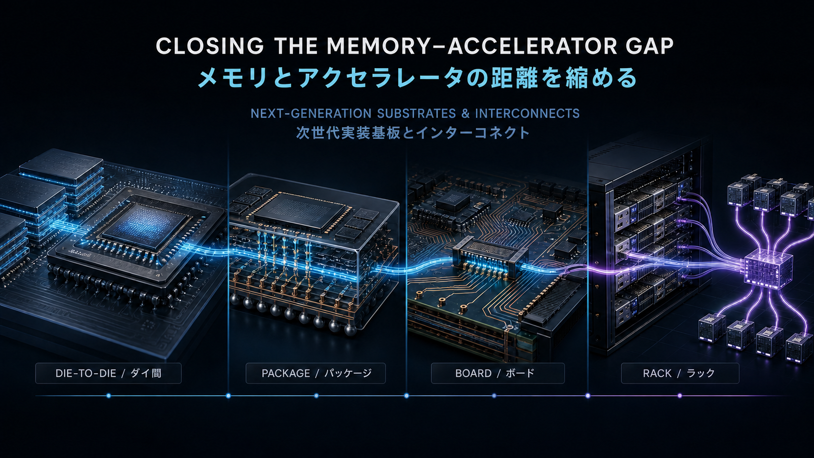
前回、メモリとアクセラレータの物理的な距離を縮める基板技術を書いたとき、Elephantech・Absolics・Eliyanという会社群を「距離を削る側」「距離を無効化する側」という軸で分類した。あの記事を書き終えてからずっと、この基板・後工程レイヤーに、実際どれだけの資金とバリュエーションの重みが乗るのかが気になっていた。8月末に出てきたサムスンの「メモリ生産能力の約70%を2031年まで長期契約(LTA)でロックした」というニュースを見た瞬間、答えの輪郭が見えた気がした。
正直に言うと、最初にこの数字を読んだときは「よくある供給逼迫の見出し」だと思って読み流しかけた。だが価格の中身を見て考えが変わった。同じ36GBのHBM3Eモジュールが、スポット市場では約2,100ドル、長期契約では約300〜400ドルで取引されている。約5倍の価格差だ。これは単なる「モノが足りない」という話ではない。誰がその5倍のスプレッドを払わされ、誰がそれを回避できるかを決める、価格の配電盤だと思う。今回はその配電盤がどこに電流(利益)を流しているのかを、後工程バリューチェーンを軸に追ってみたい。
まず数字を並べる。
| 区分 | 価格 | スポット比 |
|---|
| スポット市場 | 約287万ウォン(約2,100ドル) | 1.0倍 |
| LTA(下限) | 約50万ウォン(約300ドル) | 約0.14倍(スポットは約7倍) |
| LTA(上限) | 約70万ウォン(約400ドル) | 約0.19倍(スポットは約5倍) |
サムスンはこの価格差を武器に、メモリ生産能力の約70%を2031年までのLTAで固めた。確認できている顧客はMicrosoft・NVIDIA・Google。報道によれば、データセンター顧客5社とはすでに契約を完了し、さらに5社と最終交渉中で、その中にAmazonとMetaが含まれるという。この5社+5社という数字は一次資料で裏取りしきれていないので、あくまで「報道ベース」として扱う。
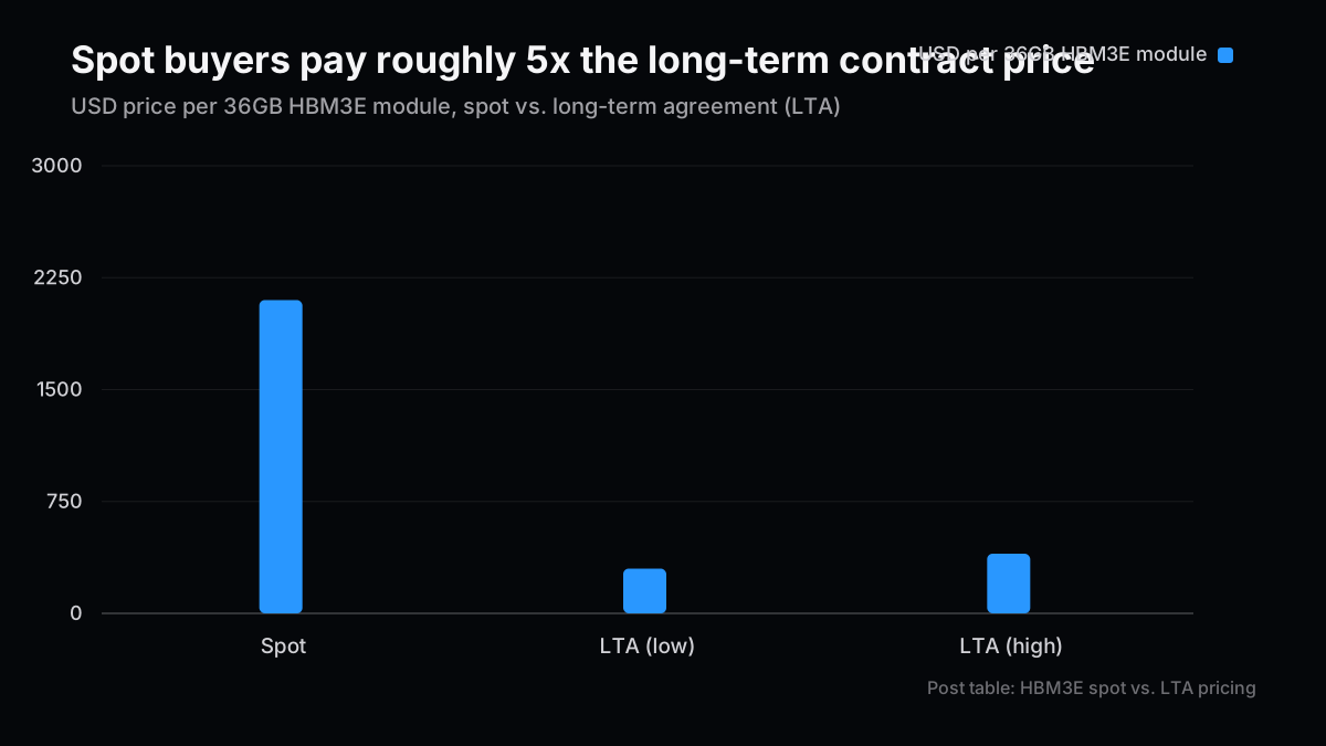
ここで立ち止まって考えたい。70%という数字そのものは、供給の何を語っているのか。 私には、供給の総量よりも「配分の固定化」を語っている数字に見える。LTAで確保できなかった買い手は、残りの30%の枠を、しかも約5倍の価格で取り合うことになる。供給が絶対的に足りないのではなく、安く買える枠が先着順で埋まっていく構造だ。これは石油の長期引取契約とスポット市場の関係に近い。量の問題である以上に、誰が先に列に並んだかという時間の問題なのだと思う。
この5倍という数字を、もう少し掘り下げる。SK Hynixは2026年分のHBM供給を「全て」売り切ったとCFOが発言し、取締役会は2031年までに54.3兆ウォン(約383億ドル)の投資を承認した。CEOは、この不足が2030年まで続きうると述べている。Micronも、HBM生産能力は2026年分まで確保済みだ。3社とも、向こう数年分の枠がすでに埋まっているという点では足並みが揃っている。
| 企業 | コミット状況 | 対象範囲・時期 | 補足 |
|---|
| サムスン | メモリ生産能力の約70%をLTAで確保 | メモリ全体、2031年まで | Microsoft・NVIDIA・Googleが確認済み顧客 |
| SK Hynix | 2026年分のHBM供給を完売(CFO発言) | HBM限定、2026年分 | 2031年までに54.3兆ウォン投資を取締役会承認済み |
| Micron | HBM生産能力を2026年分まで確保済み | HBM限定、2026年分 | インディアナ州で40億ドル規模のHBMパッケージング拠点着工(2029年生産目標はSK Hynix) |
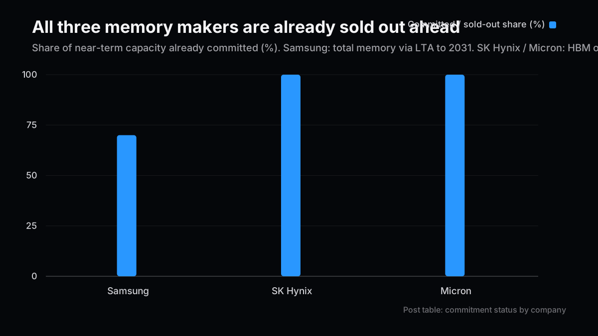
この表を見て気づいたのは、3社の「売り切れ」の意味が微妙に違うということだ。サムスンの70%はメモリ全体、SK HynixとMicronの完売はHBMに限定されている。単純に横並びで比較すると誤読する。ただ、共通しているのは、LTAで枠を取れなかった需要は、そのままスポット市場に押し出されるという構造だ。TrendForceの直近の調査では、通常のDRAM契約価格は2026年第3四半期に前四半期比13〜18%の上昇が見込まれており、サーバー向けの生産優先がPC向けDRAMの供給を圧迫していると指摘されている。HBMに割かれるウェハーが増えるほど、コモディティDRAMの側にしわ寄せが行く。この綱引きは、AI需要と消費者向けデバイスの間で、静かに、しかし確実に進んでいる。
本当にそうか、と自問してみる。──いや、もう少し正確に言えば、「サムスンの70%」という一つの数字だけを見て在庫戦略を語るのは危うい。3社のコミット状況を並べて初めて、「LTAを取れなかった買い手がどこに押し出されるか」という構造が見えてくる。数字は単体では意味を持たない。並べて初めて配管が見える、というのは前回の記事でも書いたことだが、ここでも同じだ。
ここからが、この記事で一番書きたかった部分だ。
車載EEPROMのプロセス開発をしていた頃、量産ラインである工程の歩留まりが継続的に落ちる事態に直面したことがある。現場からの一報は「装置の問題」だった。装置ベンダーを呼び、パーツを交換し、条件を出し直しても改善しない。最終的に私がTCADでプロセスウィンドウを再計算したところ、真因は装置ではなく、特定の材料ロットの組み合わせが工程マージンをぎりぎりで踏み外させていたことだった。装置は正常に動いていた。プロセスの余裕(マージン)が、想定より薄かっただけだ。
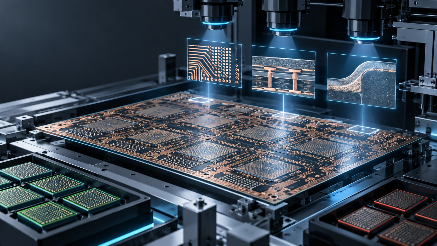
この経験が、いま議論しているHBM後工程の話とそのままつながる。SemiAnalysisの分析によれば、HBMの生産能力は今やウェハー投入量ではなくTSV(貫通シリコンビア)容量の単位で語られるようになっている。DRAMウェハーをHBMウェハーに変える工程こそが、実質的な律速段階だからだ。積層数が増えるほど歩留まりは指数関数的に悪化する——1層あたり99%の歩留まりでも、8層積層で約92%、12層積層になると約87%まで落ちる、という単純化されたモデルが紹介されている。さらに象徴的なのが、Hanmi Semiconductorのボンディング装置を巡ってSK Hynixとの間でトラブルが生じ、フィールドサービスが止まった結果、ウェハー能力は十分にあるのに生産が数か月混乱したという事例だ。装置の台数を増やすことと、実効容量が増えることは、必ずしも同じではない。 私がEEPROMの量産ラインで学んだのと同じ教訓が、桁違いの規模で繰り返されている。
この見立ての裏付けとして、実際に後工程の設備投資が動いている。Hanmi Semiconductorは2026年6月、SK HynixからHBM4向けの新型TCボンダー「TC Bonder 4.5 Griffin」を44.2億ウォンで受注し、清州のポスト・パッケージ&テスト拠点に納入する契約を結んだ。競合のASMPT・Hanwha Semitech・Kulicke & Soffaも同じ土俵でシェアを争っている。業界団体SEMIの集計では、組立・パッケージング装置の世界販売額は2026年に約70億ドル(前年比+9.2%)、2027年に約75億ドル(+6.9%)へ拡大する見通しで、テスト装置も2026年に約125億ドル(+12.0%)、2027年に約134億ドル(+7.1%)まで伸びると予測されている。AIとHBM向けの需要が、この成長の主因として名指しされている。
| レイヤー | 企業 | 直近の動き |
|---|
| TCボンダー(HBM4向け) | Hanmi Semiconductor | SK Hynixから44.2億ウォンで「TC Bonder 4.5 Griffin」を受注、清州P&T拠点向け(2026年6月) |
| TCボンダー(競合) | ASMPT・Hanwha Semitech・K&S | HBM/次世代HBFの両方でボンダー供給シェアを競う |
| 組立・パッケージング装置全体 | SEMI集計 | 2026年約70億ドル(+9.2%)、2027年約75億ドル(+6.9%)へ拡大見込み |
| テスト装置 | SEMI集計 | 2026年約125億ドル(+12.0%)、2027年約134億ドル(+7.1%)へ拡大見込み |
前回、Absolicsのガラスコア基板やElephantechの添加法配線を、「基板という受動的な脇役を能動的な設計対象に変える」動きだと書いた。今回見えてきたのは、その動きが基板だけでなく、TCボンダーやテスト装置にも同時に及んでいるということだ。ハイパースケーラー側の設備投資は、後編で示したとおり4社合計で約7,250億ドル・前年比+77%まで膨らんでいる。そのすべてがGPUに向かっているわけではなく、GPUに載せるメモリを組み立てる後工程にも、同じ勢いで資金が流れ込んでいるのだと思う。
ここまでの議論を前提に、2027年に向けたシナリオを整理する。
| シナリオ | 前提 | 価格スプレッドへの含意 | 後工程バリューチェーンへの含意 |
|---|
| ベース:緩和 | 前工程ウェハー増設と後工程(TSV・ボンディング・基板・テスト)の歩留まり立ち上げが揃って進む | スポット/LTAスプレッドが縮小 | 装置・基板各社への発注モメンタムは一服 |
| メイン:片肺増産 | ウェハー能力は積み増されるが、後工程の歩留まりとチェンジオーバーが追いつかない | スプレッドは高止まりのまま | ボンダー・TSV・基板・テスト各社への発注が続く |
| テール:需要加速 | AIデータセンター投資に加え、フィジカルAI・ヒューマノイド需要が前工程・後工程双方の増産ペースを上回る | スプレッドがさらに拡大する | 後工程装置がボトルネックの中心となり価格決定力を持つ |
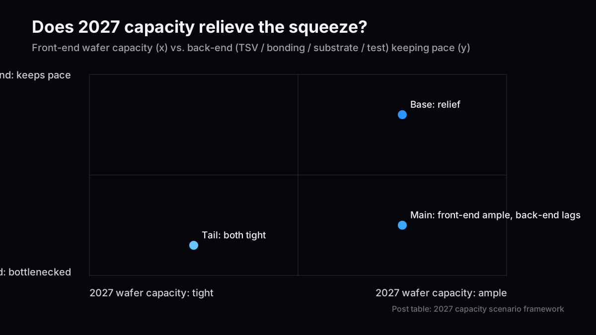
私が最も可能性が高いと見ているのは、メインシナリオだ。ウェハー投入量そのものは、サムスン・SK Hynix・Micronがそろって増設に動いている以上、2027年にかけて確実に増える。だが、TCボンダーの新規受注が2026年後半になってようやく本格化し始めた段階であることを踏まえると、ボンディング・テストという後工程側の歩留まり立ち上げが同じペースで追いつくとは考えにくい。歩留まりの立ち上げには、装置の据え付けだけでなく、プロセスウィンドウの確立と量産適用までの時間が要る。ここは私のEEPROM時代の実感とも重なる。
この見立てが崩れる条件も明示しておく。後工程装置各社(TCボンダー・テスト)の受注残高が、価格決定力の上昇を伴わずに前工程ウェハー能力と同じペースで積み上がっていることが2027年前半までに確認できれば、後工程ボトルネック仮説は弱まり、むしろ前工程のウェハー能力そのものが再びボトルネックの主役に戻る可能性が高い。逆に言えば、後工程装置各社の受注残高と単価が前工程の増設ペースを上回って伸び続ける限り、私はメインシナリオを維持する。
結論から言うと、私はこのテーマを「メモリ株を買う」という単純な話にしたくない。むしろ、前工程(ウェハー)より後工程(ボンディング・TSV・基板・テスト)の方が、利益の厚みが乗りやすい局面だと見ている。理由は単純で、前工程の増設余力は資本さえあれば比較的読みやすいのに対し、後工程の歩留まり立ち上げは資本だけでは解決しない、経験とノウハウに依存する変数だからだ。希少性は、複製しやすい側ではなく、複製しにくい側に宿る。
具体的な持ち方としては、TCボンダー・TSV関連装置・先端基板(前回扱ったAbsolicsやElephantechのような企業群)・後工程テストの4レイヤーに分散して見ていくのが妥当だと考えている。どのレイヤーも、サムスン・SK Hynix・Micronという川下の設備投資サイクルに直結しているため、川下3社のどこか一社に依存するよりもリスクが分散される。短期的にはニュートラル、中期的には後工程バリューチェーンを選別ロングというのが、今の私のスタンスだ。
次号の記事案
- 案1:TCボンダー・TSV装置株を横並びで採点する — Hanmi Semiconductor・ASMPT・Besiの受注残高と単価推移を実際の開示データで比較し、後工程ボトルネック仮説を検算する。
- 案2:HBM対コモディティDRAMのビット争奪戦を数字で追う — PC・スマートフォン向けDRAM価格の上昇ペースを、HBMへのウェハー配分シフトと突き合わせて検証する。
- 案3:サムスンの残り30%は誰が取るのか — LTA枠を取れなかった買い手のスポット調達戦略と、その企業の粗利率への影響を個社レベルで追う。
本文の事実関係と数値前提は、読者が確認できる一次情報・報道を優先して掲載している。
本記事は情報提供を目的としたものであり、特定の銘柄・企業・製品・サービスの購入や投資を推奨するものではありません。執筆者は記事内で言及した銘柄にポジションまたは利害関係を持つ可能性があります。性能値・投資額・受注額は各社の公表資料または報道ベースの数値であり、将来の成果を保証するものではありません。調査、翻訳、校正の一部に生成AIを利用していますが、最終的な内容はZYL0が確認しています。詳細は免責事項をご確認ください。
The Memory Squeeze Runs to 2031: How Samsung 70 Percent Lock-Up Rewires HBM Supply and the Back-End Value Chain
When I wrote about substrate technology closing the physical distance between memory and accelerators in a previous piece, I sorted Elephantech, Absolics, and Eliyan along a "shrinking distance versus nullifying distance" axis. Ever since finishing that post, I have kept wondering how much actual capital and valuation weight sits on that substrate-and-back-end layer. When the headline hit in late August — Samsung locking roughly 70 percent of its memory production capacity into long-term agreements (LTAs) running through 2031 — I felt like I finally had the shape of an answer.
I will admit my first reaction was to skim past it as just another supply-shortage headline. Then I looked at the actual pricing. The same 36GB HBM3E module trades for roughly $2,100 on the spot market and roughly $300 to $400 under a long-term contract — a gap of roughly five times. That is not simply a story about scarcity. It reads to me as a switchboard that decides who pays the five-times spread and who gets to avoid it. This piece follows where that switchboard actually routes the current — the profit — through the back-end value chain.
Start with the numbers as reported.
| Category | Price | Ratio to spot |
|---|
| Spot market | ~$2,100 | 1.0x |
| LTA (low end) | ~$300 | ~0.14x (spot is ~7x) |
| LTA (high end) | ~$400 | ~0.19x (spot is ~5x) |
Samsung has used that price gap as leverage to lock roughly 70 percent of its memory capacity into LTAs through 2031. Confirmed customers include Microsoft, Nvidia, and Google. Press reports say Samsung has finalized deals with five data-center customers and is in final-stage negotiation with five more, reportedly including Amazon and Meta. I could not independently verify that specific five-plus-five breakdown against a primary source, so I am treating it as press-reported rather than confirmed.
Worth pausing on this: what does the 70 percent figure actually describe? To me, it says less about total supply than about how allocation is being frozen in place. Buyers who did not get an LTA slot are left fighting over the remaining 30 percent — at roughly five times the price. This is not pure scarcity; it is a first-come, first-served structure for the cheap tranche. It resembles the relationship between long-term offtake contracts and the spot market in oil. More than a volume problem, it looks to me like a problem of who got in line first.
Push a little further into that five-times number. SK Hynix's CFO has said the company sold out its entire 2026 HBM supply, and its board approved 54.3 trillion won (roughly $38.3 billion) in investment through 2031, with the CEO saying the shortage could persist through 2030. Micron's HBM capacity is likewise booked through 2026. All three companies are effectively lined up in the same place: the next several years of allocation are already spoken for.
| Company | Commitment status | Scope / timeframe | Note |
|---|
| Samsung | ~70% of memory capacity locked via LTA | Total memory, through 2031 | Microsoft, Nvidia, Google confirmed as customers |
| SK Hynix | Entire 2026 HBM supply sold out (CFO statement) | HBM only, 2026 | Board approved 54.3T won investment through 2031 |
| Micron | HBM capacity booked through 2026 | HBM only, 2026 | Ground broken on a $4B HBM packaging facility in Indiana (SK Hynix targets 2029 output) |
What jumps out from that table is that the three companies' "sold out" statements are not measuring the same thing. Samsung's 70 percent covers total memory capacity; SK Hynix's and Micron's sellouts are scoped to HBM only. Stacking them as if they were directly comparable would be a misread. What they do share is a structural feature: demand that misses the LTA window gets pushed straight into the spot market. TrendForce's latest survey projects conventional DRAM contract prices rising 13 to 18 percent quarter over quarter in the third quarter of 2026, with server-priority production squeezing supply available for PC DRAM. The more wafers get diverted to HBM, the more the squeeze lands on commodity DRAM. That tug-of-war between AI demand and consumer devices is playing out quietly but unmistakably.
Is that really the full picture, though? Or, more precisely: reading Samsung's 70 percent in isolation and drawing inventory-strategy conclusions from it alone is risky. It is only once you line up all three companies' commitment status that the real structure appears — where demand that missed an LTA window actually gets pushed. Numbers alone rarely carry the argument; they carry it once you set them side by side, which is the same lesson I took away from the previous piece on substrates.
This is the part of the piece I most wanted to write.
Back when I was developing automotive EEPROM process technology, I once ran into a production line where yield on a particular step kept degrading. The floor report said, flatly, "equipment problem." We called in the equipment vendor, swapped parts, re-tuned process conditions — nothing improved. When I finally reran the process window in TCAD, the actual root cause was not the equipment at all: a specific combination of material lots was pushing the process margin right to its edge under certain conditions. The tool had been operating normally the entire time. The margin itself had simply been thinner than anyone assumed.
That experience maps directly onto what is happening in HBM back-end production today. According to SemiAnalysis, HBM capacity is now quoted in terms of TSV (through-silicon-via) capacity rather than raw wafer starts, because converting a DDR wafer into an HBM wafer is the real rate-limiting step. Yield degrades exponentially as layer count rises — a simplified model puts an 8-layer stack at roughly 92 percent total yield off a 99-percent-per-layer baseline, dropping to roughly 87 percent at 12 layers. The most telling illustration is a bonding-tool dispute between Hanmi Semiconductor and SK Hynix that disrupted production for months despite ample wafer capacity, once field service was withdrawn. Adding more tools and adding effective capacity are not automatically the same thing. The lesson I learned on an EEPROM line is repeating itself here, at an entirely different order of magnitude.
That read is backed by real capital deployment on the back-end side. In June 2026, Hanmi Semiconductor won a 44.2 billion won order from SK Hynix for a new TC bonder — the "TC Bonder 4.5 Griffin" — built for HBM4 and destined for SK Hynix's post-package-and-test facility in Cheongju. ASMPT, Hanwha Semitech, and Kulicke & Soffa are all competing for the same share. Industry body SEMI projects global assembly and packaging equipment sales rising to roughly $7.0 billion in 2026 (up 9.2%) and $7.5 billion in 2027 (up 6.9%), with test equipment climbing to roughly $12.5 billion in 2026 (up 12.0%) and $13.4 billion in 2027 (up 7.1%) — with AI and HBM demand named explicitly as the driver.
| Layer | Company | Recent move |
|---|
| TC bonder (HBM4) | Hanmi Semiconductor | Won a 44.2B won order from SK Hynix for the "TC Bonder 4.5 Griffin," Cheongju P&T facility (June 2026) |
| TC bonder (competitors) | ASMPT, Hanwha Semitech, K&S | Competing for bonder share across both HBM and next-gen HBF |
| Assembly & packaging, industry-wide | SEMI | Projected ~$7.0B in 2026 (+9.2%), ~$7.5B in 2027 (+6.9%) |
| Test equipment | SEMI | Projected ~$12.5B in 2026 (+12.0%), ~$13.4B in 2027 (+7.1%) |
Last time, I described Absolics' glass-core substrate and Elephantech's additive copper wiring as turning "a passive supporting substrate into an actively engineered part of the system." What has come into focus now is that the same shift is happening at the same time in TC bonders and test equipment. Hyperscaler capex, as I laid out in Part 2 of the Warsh Shock series, has swelled to roughly $725 billion combined across four companies, up 77% year over year. Not all of that flows straight into GPUs. A meaningful slice, I think, is flowing at the same pace into the back-end operations that assemble the memory those GPUs depend on.
With that groundwork laid, here is how I would frame the scenarios heading into 2027.
| Scenario | Premise | Implication for the price spread | Implication for the back-end value chain |
|---|
| Base: relief | Front-end wafer additions and back-end (TSV, bonding, substrate, test) yield ramps advance together | Spot-to-LTA spread narrows | Order momentum at equipment and substrate makers cools off |
| Main: uneven build-out | Wafer capacity is added, but back-end yield ramp and tool changeover fail to keep pace | Spread stays elevated | Orders continue flowing to bonder, TSV, substrate, and test names |
| Tail: demand accelerates further | AI data-center capex plus physical-AI and humanoid demand outrun both front-end and back-end additions | Spread widens further | Back-end equipment becomes the central bottleneck and pricing power |
The scenario I currently assign the most weight to is the main case. Wafer starts themselves will almost certainly rise into 2027, given that Samsung, SK Hynix, and Micron are all expanding in parallel. But given that new TC bonder orders only really started accelerating in the back half of 2026, it is hard for me to believe back-end yield ramp — bonding and test in particular — keeps pace with that front-end build-out. Ramping yield takes more than installing tools; it takes time to establish a process window and carry it into volume. That much overlaps directly with what I lived through in the EEPROM years.
Let me also state plainly what would change my mind. If, by the first half of 2027, back-end equipment makers' (TC bonder and test) order backlogs are shown to be climbing at the same pace as front-end wafer capacity, without an accompanying rise in pricing power, the back-end-bottleneck thesis weakens, and front-end wafer capacity itself likely becomes the dominant constraint again. Conversely, as long as back-end equipment makers' order backlogs and unit pricing keep outrunning the pace of front-end expansion, I will hold the main scenario.
My conclusion is that I do not want to reduce this theme to "buy memory stocks." I would rather frame it as: the back end (bonding, TSV, substrate, test) is more likely than the front end (wafer) to carry a thicker margin through this cycle. The reasoning is straightforward. Front-end capacity expansion is comparatively forecastable — if you have the capital, you can plan the build-out. Back-end yield ramp does not resolve with capital alone; it depends on process know-how and experience, which is a much harder variable to buy your way past. Scarcity concentrates on the side that is hard to replicate, not the side that is easy to copy.
Concretely, I think it makes sense to spread exposure across four layers: TC bonders, TSV-related equipment, advanced substrates (the same Absolics- and Elephantech-type names from the previous piece), and back-end test. Every one of those layers sits directly downstream of the capex cycles at Samsung, SK Hynix, and Micron, which spreads out the risk of depending on any single one of the three. My current stance is neutral in the near term and selectively long the back-end value chain over the medium term.
Next Issue Ideas
- Idea 1: Scoring TC bonder and TSV equipment names side by side — Compare disclosed order backlogs and unit pricing at Hanmi Semiconductor, ASMPT, and Besi to stress-test the back-end-bottleneck thesis with real data.
- Idea 2: Tracking the HBM vs. commodity DRAM bit fight in numbers — Cross-reference PC and smartphone DRAM price momentum against the pace of wafer reallocation toward HBM.
- Idea 3: Who gets Samsung's remaining 30 percent — Follow the spot-buying strategies of customers that missed the LTA window, and how it hits their gross margins at the single-name level.
Facts and figures in this piece prioritize primary and official sources readers can verify themselves.
This article is for informational purposes only and does not constitute investment advice or a recommendation to buy any specific stock, company, product, or service. The author may hold positions or have interests in the names discussed. Performance figures, investment amounts, and order values are vendor-reported or press-reported and do not guarantee future results. Generative AI was used for parts of the research, translation, and proofreading, but the final content has been reviewed by ZYL0. See the disclaimer for details.