半導体×VCの勝ち筋は「ボラティリティを設計する」こと
私は半導体プロセス開発の現場でEEPROMの量産化と歩留まり改善を主導してきた人間です。半導体産業の「サイクリカル性」は教科書の話ではなく、4製品以上の量産立ち上げを通じて骨で覚えた肌感覚です。サイクルの波に乗るのは難しいが、サイクルを無効化する構造的ポジションは取れる——これがTier1 VCの戦略を10年見続けて私が至った結論で、連載最終回はその視点で全体を統合します。
最初に、本連載の問題意識をフラットに置きます。
半導体産業は本質的にサイクリカルです。需要は爆発的に膨らみ、供給は2〜3年後に追いつき、価格は暴落する——半導体の歴史はその繰り返しでした。しかし今、Tier1 VCが半導体スタートアップに数億ドルを投じるとき、彼らは「サイクルの波に乗る」のではなく、「サイクル自体を無効化する構造的ポジション」を狙っています。
それが「ボラティリティを設計する(designing for volatility)」という概念です。チップの価格が上下しても需要が安定する「標準化されたインターフェース技術」(CPO、UCIeなど)、チップ世代交代のたびに価値が高まる「設計インフラ」(EDA自動化、IP再利用)、特定のハードウェアベンダーに依存しない「ソフトウェア定義の計算基盤」——いずれも、価格競争に巻き込まれにくいレイヤーへの賭けです。
本連載の最終回では、連載①②で整理したVCの戦略・技術・案件データを踏まえ、以下を体系化します。
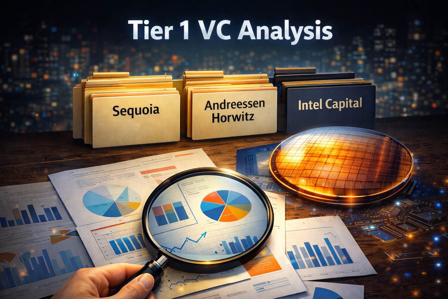
- Tier1 VC 5社の戦略比較と差異の本質
- 短期(〜18ヶ月)・中期(2〜4年)・長期(5年〜)の投資機会とリスク
- マクロ環境(市場規模・装置投資・政策)のサマリ
- 個人投資家・機関投資家・事業会社それぞれへの示唆

①「AI需要→半導体ボトルネック→スタートアップ機会」という構造は2026年以降も継続する
GPU性能のスケーリングが続く限り、設計・データ移動・パッケージングというボトルネックは解消されない。Tier1 VCはこの構造的需要を見越し、すでに2023〜2025年に大型投資を実行済みなんですよね。
②VC各社の"賭け方"は大きく異なる:エコシステム型 vs. 垂直統合型
Sequoia・a16zがスタートアップ群への分散投資でエコシステムを形成するのに対し、SoftBankはAmpere($6.5B評価額)など垂直統合型の大型単独案件を選好します。Kleiner PerkinsはIPO経路を重視した米国製造復活テーマに集中し、Bessemerはデータセンターインフラとのシナジーを軸に据える。
③長期は「新計算原理」が最大の非線形リターン源だが、商用化リスクは高い
アナログ計算・量子・フォトニクスはいずれも現在の投資期待値が低い一方、商用化に成功した場合のリターンは既存手法と非線形に差がつく。VCはこれらをポートフォリオの「オプション」として保有し、中期の確実な案件でポートフォリオを安定させる戦略をとっています。
| VC | 投資の"型" | 代表案件 | 提携・エコシステム構造 | 想定出口 |
|---|
| Sequoia Capital | 分散・エコシステム型。設計自動化・新計算原理を中心に複数スタートアップへ初期投資 | Ricursive ($35M)、Unconventional Computing ($475M) | NVIDIA・Synopsys・Coreweaveとのネットワークで被投資企業を繋ぐ | M&A(EDA大手)またはIPO(計算インフラ) |
| Andreessen Horowitz (a16z) | テーマ型・大型集中。「AIファクトリー」インフラを横断するデータ移動と新世代メモリ | Ayar Labs ($500M)、Nexthop AI ($500M) | クラウドプロバイダー(AWS・Azure・GCP)とのコマーシャルパイプライン形成 | データセンター事業者へのM&AまたはIPO |
| Kleiner Perkins | 政策・製造復活テーマ型。CHIPS法補助金の受益企業、米国製造回帰 | Retym ($75M)、Kandou Technologies ($92.3M) | SEMI協会・米国防総省DARPAプログラムとの連携 | IPO(CHIPS法関連企業への市場期待) |
| Bessemer Venture Partners | データセンターインフラ連動型。既存クラウド投資との シナジーを重視 | Quantum Circuits ($60M+)、ChipAgents ($21M) | 既存クラウド・SaaS投資先との顧客共有 | M&A(クラウド大手による内製化) |
| SoftBank Vision Fund | 垂直統合・メガラウンド型。単一企業に大規模資本を集中、グループ内シナジー優先 | Ampere Computing ($6.5B評価額)、Graphcore買収 | SBグループ(ARM・T-Mobile・WeWork残存網)との垂直統合 | 長期保有またはIPO(ARM上場の先例) |
エコシステム型(Sequoia / a16z / KP / Bessemer)
────────────────────────────────────────────
VC
 ├── スタートアップA(設計)
 ├── スタートアップB(インターコネクト)
 ├── スタートアップC(パッケージング)
 └── スタートアップD(新計算)
        │
        ▼
 各社が相互に顧客・サプライヤー関係を形成
 → VC自身がエコシステムのハブになる

垂直統合型(SoftBank)
────────────────────────────────────────────
SoftBank
 └── Ampere Computing(独自Arm CPU設計)
      └── ARM(SB傘下)からIPライセンス
           └── データセンター向け直販モデル
                → グループ内でValue Chainを完結
| 機会領域 | 投資テーマ | 代表スタートアップ | 主なリスク |
|---|
| EDA自動化 | LLMによる回路検証・バグ修正の自動化で設計期間を30〜50%短縮 | Ricursive(Seq.)、ChipAgents(Bessemer) | Synopsys/Cadenceがin-house LLM開発を加速、M&Aで吸収する可能性 |
| IP再利用・モジュール化 | 既存IP資産のAI検索・カスタマイズにより新チップ設計コスト削減 | 複数の非公開ステルス案件 | 大手ファブ(TSMC・Samsung)が独自IPライブラリを強化、差別化困難 |
| サプライチェーン可視化 | 地政学リスクにより部品調達の不確実性が増大、可視化SaaSへの需要急増 | (非公開多数) | 景気後退局面ではソフトウェア支出が最初に削減される |
短期の投資判断基準:収益化期間が短い(18ヶ月以内に初期顧客獲得可能)か、規制の影響を受けにくいソフトウェアファーストモデルかどうかが鍵。EDA自動化はこの条件を満たすが、競合(Cadence・Synopsys)の大型R&D予算には要注意。
| 機会領域 | 投資テーマ | 代表スタートアップ | 主なリスク |
|---|
| CPO(コパッケージド光学) | GPU-メモリ間の銅配線を光配線に置換、帯域幅を10倍・消費電力を60〜80%削減 | Ayar Labs(a16z、$500M) | 量産歩留まり(光コンポーネントの製造難易度)、TSMC/IntelのCPO内製化リスク |
| 高速SerDes・電気インターコネクト | 銅配線の延命技術としてデータセンター内配線を高効率化 | Kandou Technologies(KP、$92.3M) | 光学への移行が予想より早まった場合のレガシー化リスク |
| 先端パッケージング(Chiplet/3D IC) | Chiplet標準規格(UCIe)による異種チップ統合 | Nexthop AI(a16z、$500M) | ファブレスとファブの間のIP所有権交渉の複雑化 |
| 次世代メモリインターフェース | HBM3/4の後継として帯域幅と電力効率のトレードオフを再設計 | (SK Hynix・Micronとの協業スタートアップ) | DRAMメーカーの自社開発能力向上でサードパーティ不要論 |
中期の投資判断基準:TSMC・Samsung・Intelの先端パッケージング拡張計画と競合するかどうか。競合するなら提携関係(JDA)を確立できているかが生死を分ける。Ayar Labsがa16zの支援のもとTSMCと共同開発体制を構築しているのはこの典型例。
| 機会領域 | 投資テーマ | 代表スタートアップ | 主なリスク |
|---|
| アナログ計算 | デジタル変換コストを排除し推論電力を100分の1以下に削減、エッジAI向け | Unconventional Computing(Seq.、$475M) | プログラマビリティ(汎用性)の制限、開発者エコシステムの未成熟 |
| 量子コンピューティング | 素因数分解・量子化学シミュレーション・最適化問題での超越性 | Quantum Circuits(Bessemer、$60M+)、Rigetti($79M) | エラー訂正技術の成熟度、「量子優位性」の商用ユースケース特定 |
| フォトニック計算 | 光を用いた行列演算でAI推論の消費電力を抜本的に削減 | (非公開複数社) | シリコンフォトニクスの製造インフラ未成熟、スケールアップコスト |
| ニューロモルフィック | 脳の神経回路を模倣した非同期計算、超低電力センサー処理 | (学術スピンアウト複数) | 汎用計算への転用困難、ニッチ市場からの脱出経路不明確 |
長期の投資判断基準:「論文→プロダクト→市場」の接続性。量子の場合、論文数と特許出願は世界トップクラスだが、商用ユースケースへの接続(特にエラー率の商用許容水準到達)が見えていない企業は評価を保留すべきなんですよね。一方、アナログ計算はエッジ推論という明確な市場セグメントが存在し、中期以降の商用化シナリオが描きやすい。
| 指標 | 2024実績 | 2025予測 | 2026予測 | 2027予測 | 出典 |
|---|
| 世界半導体市場規模 | $627B | $791.7B | $975B | $1.1T+ | WSTS 2025年秋季予測 |
| 300mm装置支出 | $107B | $119B | $133B | $151B | SEMI 2026年予測 |
| AI半導体(GPU/NPU/ASIC) | $130B | $200B+ | $280B+ | $380B+ | IDC/Gartner各社推計 |
| 米CHIPS法補助金執行額 | $8B | $30B+ | $52B(総額上限) | 〃 | 米商務省 |
| 中国半導体輸出規制強化 | HBM・EDA規制 | EUV輸出制限継続 | さらなる強化見込み | 〃 | BIS/経産省 |
CHIPS法・EU半導体法
    │
    ├── 補助金の受益企業(Intel Foundry・TSMC米国拠点・Samsung Texas)
    │        └── → 建設・装置・材料スタートアップに間接需要
    │
    └── 地政学リスクの優先度上昇
             └── → 米国内設計・製造のスタートアップへのVC資金流入加速

中国規制(BIS 輸出規制)
    │
    ├── 中国向けAI半導体(H800→H20)の販売制限
    │        └── → 中国内半導体自給自足投資の爆発(华为/寒武纪等)
    │
    └── 先進EDA・製造装置の中国輸出禁止
             └── → 欧米スタートアップへの反射的恩恵(競合中国企業の能力制限)
Tier1 VCの実際のポートフォリオ配分から読み取れるのは、以下のような「時間軸別の3層構造」だ:
ポートフォリオの理想的な時間軸配分(イメージ)
─────────────────────────────────────
短期(〜18ヶ月)  ████████████████░░░░  40%
  └── EDA自動化・設計SaaS・サプライチェーン可視化

中期(2〜4年)    ██████████████████░░  45%
  └── CPO・インターコネクト・先端パッケージング・AIアクセラレータ

長期(5年〜)     ██████░░░░░░░░░░░░░░  15%
  └── アナログ計算・量子・フォトニクス・ニューロモルフィック
─────────────────────────────────────
個人投資家が直接VCファンドに参加できるケースは限られるが、以下の方法で間接的な半導体スタートアップエクスポージャーを取得できる:
- 上場半導体企業(NVIDIA・ASML・Lam Research・TSMC ADR):スタートアップの顧客であり、スタートアップが解決するボトルネックから直接利益を得る
- 半導体特化ETF(SOXX・SMH):分散効果はあるが、大型株中心でスタートアップの成長性は反映されにくい
- SPAC・二次流通市場:Rigetti(量子)のようにSPAC経由で上場した銘柄は、高リスク・高ボラティリティで個人投資家がアクセスしやすい
- CVCを持つ事業会社株:SoftBankグループ・Intel Capital・Qualcomm Ventures母体企業への投資は、VCポートフォリオへの間接アクセスとなる
- LP(大学基金・年金):Sequoia / a16z / Bessemerへのコミットメントは半導体の長期テーマと合致するが、J-Curveリスク(投資後3〜5年はリターンがマイナス)を許容できる長期資金が前提
- 事業会社CVC:自社バリューチェーンのボトルネックを特定し、そこに対応するスタートアップへ戦略的投資することで、M&Aオプションと市場情報を同時に取得できる
| 連載 | 核心メッセージ |
|---|
| 連載①:概観と主要プレイヤー | Tier1 VCは「AI需要のボトルネック」という構造的欠如部分に集中している。チップ単体ではなく、設計・移動・実装・供給網という4層への分解投資が共通パターン |
| 連載②:技術別ケーススタディ | EDA自動化・CPO・先端パッケージング・新計算原理という4領域で約$2.5B規模の投資が2022〜2025年に集中執行された。技術的成熟度と商用化パスが投資規模を決定している |
| 連載③:戦略的示唆(本稿) | VCの「型」はエコシステム型と垂直統合型に二分される。短期はソフトウェア収益性、中期はCPO/パッケージング、長期はアナログ・量子がそれぞれのリターン源 |
- Ayar Labs量産開始タイミング:a16zが$500M投じたCPOの量産が2026〜2027年に本格化するか。歩留まりが商用水準(90%以上)に達するかが業界全体のCPO移行速度を決定する
- Ampere ComputingのIPO計画:SoftBankが2026年中に示唆しているAmpereのIPOが実現すれば、Arm系CPUのデータセンター向け市場シェアの公開データが初めて入手可能になる
- CHIPS法補助金の第2フェーズ:2026年後半に予定される米商務省の第2ラウンド補助金決定(ファウンドリー以外の設計・材料・EDA企業への配分拡大)が、スタートアップへの資金流入を加速させる可能性がある
- 中国の先進ファブリケーション突破口:HuaweiのKirin/Ascend系チップが7nm相当に到達した実績を踏まえ、5nm以下への突破タイミングが欧米規制強化の速度と「技術ギャップ」の行方を決める
- 量子エラー訂正の商用許容水準到達:Google(Willow)・IBM・Microsoftが競う論理量子ビットの実装が2027〜2028年に商用ユースケース(金融最適化・創薬)に接続できるか
半導体投資の本質は「インフラのロックイン」です。GPUもメモリも、単体では差別化できない。しかし、その間をつなぐデータ移動技術(CPO・SerDes)、上流の設計効率(EDA自動化)、下流の実装技術(先端パッケージング)は、一度採用されたらすぐには切り替えられない粘着性(スティッキネス)を持ちます。
Tier1 VCがこの領域に$2.5B以上を集中させているのは、「チップの価格競争に巻き込まれたくない」という合理的判断の結果です。価格競争は製造業の宿命だが、インフラはソフトウェア的なネットワーク効果を持てる——これは、私が現場で量産プロセスのコモディティ化と「装置・データ・プロセスIP」の固有価値を同時に経験してきたからこそ、強く同意できる構造です。
連載を通じて改めて感じたのは、「半導体は地政学と分離できない」という事実。CHIPS法・BIS輸出規制・日本の経済安保法——これらの政策変数が、純粋な技術評価と同等以上に投資判断を左右します。個人投資家として半導体セクターに向き合うなら、技術だけでなく政策カレンダーを同時に追うことが不可欠だと考えています。
- 案1:数字で追う続編 — 本記事の前提を最新データで更新し、何が強まり、何が崩れたかを再点検する。
- 案2:実務テンプレート編 — 読者が自分の投資判断、制作単価、または開発運用に転用できるチェックリストへ落とし込む。
- 案3:反対シナリオの検証 — 今回の見立てが外れる条件を先に定義し、次に見るべき指標と時間軸を整理する。
本文の事実関係と数値前提は、再審査時にも読者が確認できる一次情報・公的資料を優先して見直しています。
本記事は情報提供を目的としたものであり、特定の銘柄、サービス、契約条件の推奨や投資助言ではありません。執筆者は記事内で触れた銘柄やサービスにポジションまたは利害関係を持つ可能性があります。調査、翻訳、校正の一部に生成AIを利用していますが、最終的な内容はZYL0が確認しています。詳細は免責事項をご確認ください。
Semiconductor VC: Designing for Volatility
I came up through the floor — leading EEPROM volume production and yield improvement on the process side. Semiconductor cyclicality isn't a textbook abstraction for me; it's something I felt in my bones across more than four product ramps. You can't reliably surf the cycle, but you can take structural positions that are immune to it. That's the conclusion I've arrived at after watching Tier-1 VCs for a decade, and that's the lens that ties this final installment together.
Let me reset the question flat first.
The semiconductor industry is inherently cyclical. Demand explodes, supply catches up 2–3 years later, prices collapse — the history of semiconductors has always been one of boom and bust. But when Tier-1 VCs commit hundreds of millions of dollars to semiconductor startups today, they are not trying to "ride the cycle." They are targeting structural positions that are immune to the cycle itself.
This is what "designing for volatility" means: investing in standardized interface technologies (CPO, UCIe) whose demand remains stable even when chip prices swing wildly; design infrastructure (EDA automation, IP reuse) that becomes more valuable with every chip generation transition; and software-defined computing foundations that are independent of any specific hardware vendor — bets on layers where price competition doesn't dominate.
In this final installment, I synthesize the strategy, technology, and deal data from Parts 1 and 2 into four key frameworks:
- Comparative analysis of five Tier1 VCs and the essence of their strategic differences
- Investment opportunities and risks across short (≤18 months), medium (2–4 years), and long (5+ years) time horizons
- Macro environment summary: market size, equipment investment, and policy
- Implications for individual investors, institutional investors, and corporate strategists
① The "AI demand → semiconductor bottleneck → startup opportunity" structure will persist beyond 2026
As long as GPU performance scaling continues, bottlenecks in design, data movement, and packaging will remain unsolved. Tier1 VCs have already anticipated this structural demand with major investments executed in 2023–2025.
② VC firms' investment "styles" diverge sharply: ecosystem model vs. vertical integration model
While Sequoia and a16z build ecosystems through diversified investments in startup clusters, SoftBank concentrates capital in large single-company vertical integration bets (e.g., Ampere at $6.5B valuation). Kleiner Perkins focuses on the U.S. manufacturing revival thesis with clear IPO paths, while Bessemer emphasizes synergies with its existing data center infrastructure portfolio.
③ Long-term, "new computing paradigms" offer the highest non-linear return potential — but commercialization risk is high
Analog computing, quantum, and photonics all carry low near-term expected values, but successful commercialization creates non-linear return gaps versus conventional approaches. VCs hold these as "options" within diversified portfolios, using medium-term certainties to stabilize overall returns.
| VC | Investment Style | Signature Deals | Ecosystem/Partnership Structure | Expected Exit |
|---|
| Sequoia Capital | Diversified ecosystem. Early-stage bets across design automation and novel computing paradigms | Ricursive ($35M), Unconventional Computing ($475M) | Network bridges portfolio companies to NVIDIA, Synopsys, Coreweave | M&A (EDA majors) or IPO (compute infra) |
| Andreessen Horowitz (a16z) | Thematic, large concentrated bets on "AI factory" infrastructure spanning data movement and next-gen memory | Ayar Labs ($500M), Nexthop AI ($500M) | Commercial pipeline formation with cloud providers (AWS, Azure, GCP) | M&A by data center operators or IPO |
| Kleiner Perkins | Policy/manufacturing revival theme. CHIPS Act beneficiaries, U.S. onshoring thesis | Retym ($75M), Kandou Technologies ($92.3M) | SEMI association, U.S. DoD/DARPA program linkages | IPO (market enthusiasm for CHIPS Act beneficiaries) |
| Bessemer Venture Partners | Data center infrastructure synergy. Prioritizes fit with existing cloud investment portfolio | Quantum Circuits ($60M+), ChipAgents ($21M) | Customer sharing with existing cloud/SaaS portfolio companies | M&A (cloud majors internalizing capabilities) |
| SoftBank Vision Fund | Vertical integration, mega-rounds. Concentrated capital in single companies; group synergy prioritized | Ampere Computing ($6.5B valuation), Graphcore acquisition | Vertical integration with SB group (Arm, T-Mobile, residual WeWork network) | Long-term hold or IPO (Arm IPO as precedent) |
Ecosystem Model (Sequoia / a16z / KP / Bessemer)
────────────────────────────────────────────────
VC
 ├── Startup A (Design Automation)
 ├── Startup B (Interconnect/CPO)
 ├── Startup C (Advanced Packaging)
 └── Startup D (New Computing Paradigm)
        │
        ▼
 Portfolio companies form mutual customer-supplier relationships
 → VC itself becomes the hub of a self-reinforcing ecosystem

Vertical Integration Model (SoftBank)
────────────────────────────────────────────────
SoftBank
 └── Ampere Computing (proprietary Arm CPU design)
      └── IP licensed from Arm (SB subsidiary)
           └── Direct-to-data-center sales model
                → Full value chain captured within the group
| Opportunity | Investment Theme | Representative Startups | Key Risks |
|---|
| EDA Automation | LLM-powered circuit verification and bug correction reducing design time by 30–50% | Ricursive (Seq.), ChipAgents (Bessemer) | Synopsys/Cadence accelerating in-house LLM development; acquisition risk |
| IP Reuse/Modularization | AI-powered search and customization of existing IP assets reducing new chip design cost | Multiple undisclosed stealth-stage companies | Leading fabs (TSMC, Samsung) building proprietary IP libraries, crowding out differentiation |
| Supply Chain Visibility | Geopolitical risk driving demand for SaaS platforms that map procurement uncertainty | (Numerous undisclosed companies) | In a recession, software spend is the first to be cut |
Short-term investment criteria: Can the company acquire initial customers within 18 months? Is the model software-first and insulated from regulatory risk? EDA automation meets these conditions, but the large R&D budgets of Cadence and Synopsys demand constant vigilance.
| Opportunity | Investment Theme | Representative Startups | Key Risks |
|---|
| CPO (Co-Packaged Optics) | Replacing copper GPU-to-memory interconnect with optical fiber; 10× bandwidth, 60–80% power reduction | Ayar Labs (a16z, $500M) | Production yield (optical component manufacturing complexity); TSMC/Intel CPO internalization risk |
| High-Speed SerDes and Electrical Interconnect | Extending copper's lifespan by improving intra-data-center wiring efficiency | Kandou Technologies (KP, $92.3M) | Legacy risk if optical migration happens faster than expected |
| Advanced Packaging (Chiplet/3D IC) | Heterogeneous chip integration via Chiplet standards (UCIe) | Nexthop AI (a16z, $500M) | IP ownership negotiation complexity between fabless companies and foundries |
| Next-Gen Memory Interfaces | Redesigning bandwidth vs. power tradeoffs as HBM3/4 successors | (Startups co-developing with SK Hynix, Micron) | DRAM vendors' growing in-house development capacity making third parties redundant |
Medium-term investment criteria: Does the company compete with TSMC's, Samsung's, or Intel's advanced packaging expansion plans? If so, has it established a JDA (Joint Development Agreement) partnership? This is a matter of survival. Ayar Labs' co-development structure with TSMC, backed by a16z, is the canonical example.
| Opportunity | Investment Theme | Representative Startups | Key Risks |
|---|
| Analog Computing | Eliminating digital conversion overhead; 100× inference power reduction for edge AI | Unconventional Computing (Seq., $475M) | Programmability (generality) limitations; underdeveloped developer ecosystem |
| Quantum Computing | Exceeding classical computation in prime factorization, quantum chemistry simulation, optimization | Quantum Circuits (Bessemer, $60M+), Rigetti ($79M) | Error correction maturity; identifying commercial use cases that achieve "quantum advantage" |
| Photonic Computing | Using light for matrix operations to dramatically reduce AI inference power consumption | (Multiple undisclosed companies) | Immature silicon photonics manufacturing infrastructure; scale-up cost |
| Neuromorphic Computing | Asynchronous computation mimicking neural circuits; ultra-low-power sensor processing | (Multiple academic spinouts) | Difficult to adapt for general-purpose compute; unclear path from niche markets |
Long-term investment criteria: Is there a clear "paper → product → market" connection? For quantum, the volume of papers and patents is world-class, but companies that cannot show a path to commercial error rates should be approached with caution. Analog computing, by contrast, has a well-defined target market in edge inference, making medium-to-long-term commercialization scenarios more legible.
| Metric | 2024 Actual | 2025 Forecast | 2026 Forecast | 2027 Forecast | Source |
|---|
| Global Semiconductor Market | $627B | $791.7B | $975B | $1.1T+ | WSTS Autumn 2025 |
| 300mm Equipment Spending | $107B | $119B | $133B | $151B | SEMI 2026 Forecast |
| AI Semiconductors (GPU/NPU/ASIC) | $130B | $200B+ | $280B+ | $380B+ | IDC/Gartner estimates |
| U.S. CHIPS Act Grants Executed | $8B | $30B+ | $52B (cap) | — | U.S. Commerce Dept. |
| China Semiconductor Export Controls | HBM + EDA | EUV export ban continues | Further tightening expected | — | BIS/METI |
CHIPS Act / EU Chips Act
    │
    ├── Direct beneficiaries (Intel Foundry, TSMC Arizona, Samsung Texas)
    │        └── → Indirect demand for construction/equipment/materials startups
    │
    └── Elevated priority on geopolitical risk management
             └── → Accelerated VC capital flow into U.S.-designed/manufactured startups

China Export Controls (BIS)
    │
    ├── Sales restrictions on AI chips to China (H800 → H20)
    │        └── → China's domestic semiconductor self-sufficiency investment explodes (Huawei/Cambricon)
    │
    └── Advanced EDA/equipment export ban to China
             └── → Reflexive benefit for Western startups (Chinese competitors' capability constrained)
Reading across the actual portfolio allocations of Tier1 VCs reveals a consistent three-layer structure by time horizon:
Ideal Portfolio Allocation by Time Horizon (Illustrative)
──────────────────────────────────────────────────────
Short-term (≤18 months)   ████████████████░░░░  40%
  └── EDA automation · Design SaaS · Supply chain visibility

Medium-term (2–4 years)   ██████████████████░░  45%
  └── CPO · Interconnect · Advanced packaging · AI accelerators

Long-term (5+ years)      ██████░░░░░░░░░░░░░░  15%
  └── Analog computing · Quantum · Photonics · Neuromorphic
──────────────────────────────────────────────────────
Individual investors rarely have direct access to VC funds, but indirect semiconductor startup exposure is available through:
- Listed semiconductor companies (NVIDIA, ASML, Lam Research, TSMC ADR): Direct customers of startups, benefitting directly from the bottlenecks that startups are solving
- Semiconductor ETFs (SOXX, SMH): Diversification benefit, but large-cap weighted — limited startup growth reflection
- SPACs and secondary markets: Companies like Rigetti (quantum), which went public via SPAC, offer individual investors high-risk, high-volatility access
- Corporate parents of active CVCs: Investing in SoftBank Group, Intel (Intel Capital parent), or Qualcomm (Qualcomm Ventures parent) provides indirect VC portfolio exposure
- LPs (endowments, pension funds): Commitments to Sequoia / a16z / Bessemer align well with long-term semiconductor themes, but require capital that can tolerate the J-Curve (returns typically negative for 3–5 years post-commitment)
- Corporate CVC: Identify the bottleneck in your own value chain and strategically invest in the startup addressing it — simultaneously acquiring M&A optionality and competitive intelligence
| Part | Core Message |
|---|
| Part 1: Overview and Key Players | Tier1 VCs are concentrating on the "structural absence" at AI infrastructure bottlenecks. The common pattern is decomposing investment across four layers — design, movement, packaging, and supply chain — rather than betting on chips themselves |
| Part 2: Technology Deep Dives | Approximately $2.5B in investment was concentrated across EDA automation, CPO, advanced packaging, and new computing paradigms from 2022–2025. Technical maturity and commercial path clarity determine deal size |
| Part 3: Strategic Implications (this piece) | VC styles bifurcate into ecosystem vs. vertical integration models. Short-term returns come from software profitability; medium-term from CPO/packaging; long-term from analog/quantum |
- Ayar Labs volume production timeline: Will a16z's $500M CPO bet reach volume manufacturing in 2026–2027? Achieving commercial yield rates (90%+) will determine the pace of CPO adoption across the entire industry
- Ampere Computing IPO: If SoftBank's hinted 2026 IPO for Ampere materializes, it will provide the first publicly available data on Arm-based CPU market share in data centers
- CHIPS Act Phase 2 grants: U.S. Commerce Department's second-round grant decisions in H2 2026 (expanding beyond foundries to design, materials, and EDA companies) could accelerate capital flows to startups
- China's advanced fabrication breakthrough: Given Huawei's demonstrated 7nm-equivalent Kirin/Ascend chips, the timing of any sub-5nm breakthrough will determine both Western regulatory response speed and the persistence of the "technology gap"
- Quantum error correction hitting commercial tolerances: Whether Google (Willow), IBM, and Microsoft's logical qubit implementations can connect to commercial use cases (financial optimization, drug discovery) by 2027–2028
The essence of semiconductor investment is infrastructure lock-in. GPUs alone, memory alone — neither creates sustainable differentiation. But the data-movement technology bridging them (CPO, SerDes), the upstream design-efficiency layer (EDA automation), and the downstream assembly layer (advanced packaging) all have the kind of stickiness that resists easy substitution once adopted.
Tier-1 VCs concentrating $2.5B+ in these areas is the rational outcome of a simple observation: they don't want to be dragged into chip price competition. Price wars are manufacturing's destiny, but infrastructure can achieve software-like network effects. From having watched the same dynamic play out in process IP, equipment data, and yield-improvement know-how on the floor, I think this framing is right.
What this series reinforced for me is that semiconductors are inseparable from geopolitics. The CHIPS Act, BIS export controls, Japan's economic security legislation — these policy variables influence investment decisions at least as much as pure technical assessment.
For individual investors engaging with the semiconductor sector: tracking the policy calendar alongside the technology roadmap is no longer optional. It's table stakes.
- Idea 1: A data-updated follow-up — Revisit the thesis with fresh numbers and separate what strengthened from what broke.
- Idea 2: A practical template edition — Turn the article into a checklist readers can reuse for investing, pricing, or technical operations.
- Idea 3: The bear-case test — Define the conditions that would invalidate this view and map the indicators to watch next.
- Semiconductor VC Series①: Converging on AI Bottlenecks — Where are Tier-1 VCs placing bets in the expanding $975B semiconductor market? Strategies of Sequoia, a16z, Kleiner Pe…
- Why Design, Data Movement & Packaging Attract VC Capital — Series② — As GPU performance scales, design, I/O, and packaging become the real AI bottleneck.
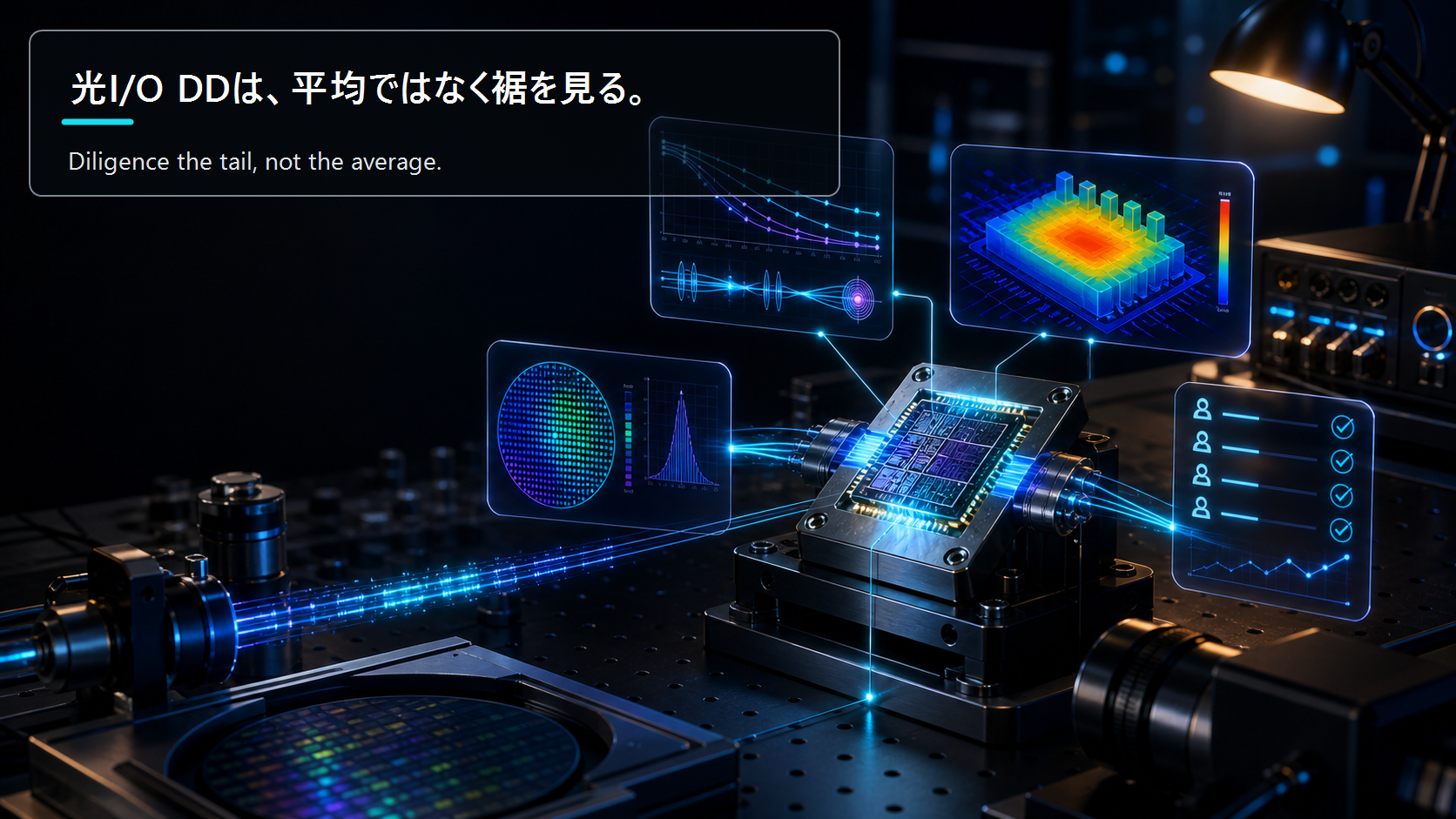
- How to Diligence Optical I/O Startups: Measuring Insertion Loss, Thermals, Manufacturability, and Customer Validation — A CVC diligence checklist for optical I/O startups: pressing insertion loss, thermals, manufacturing yield, and custom…
The factual and numerical assumptions in this article are anchored to primary or public materials that readers can revisit during AdSense review and future updates.
This article is for informational purposes only and does not constitute investment advice or a recommendation of any specific stock, service, or contract structure. The author may hold positions or interests related to companies or services mentioned. Generative AI was used for parts of research, translation, and proofreading, with final review by ZYL0. See the disclaimer for details.