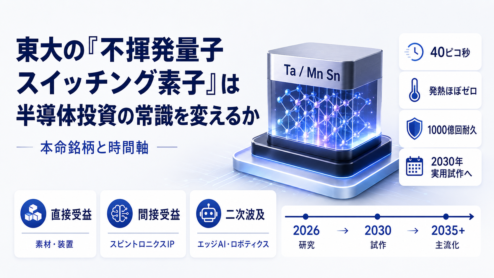
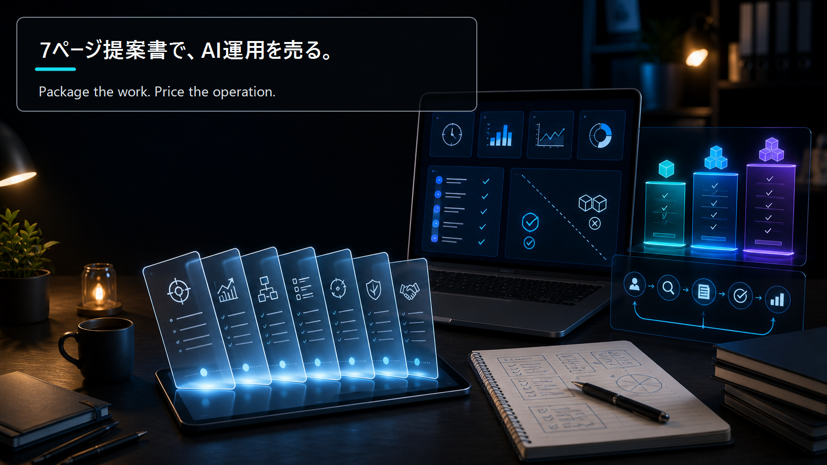
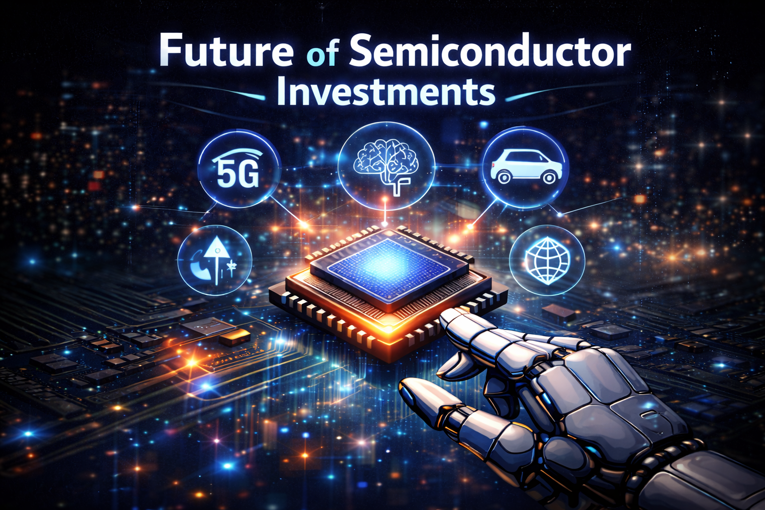
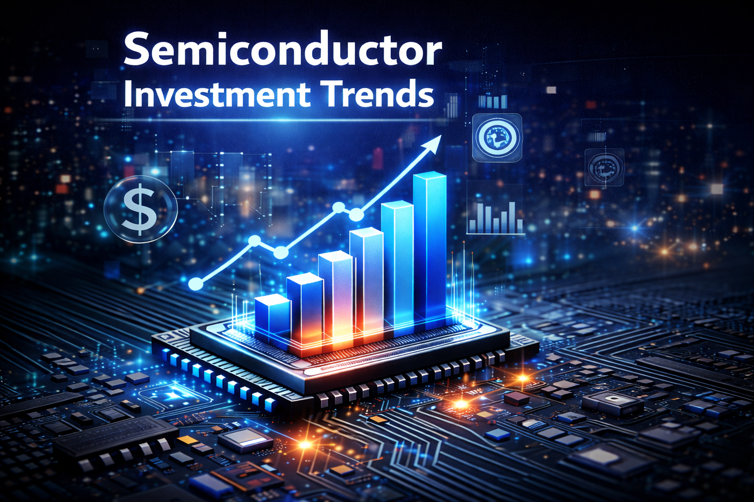
東大の「不揮発量子スイッチング素子」は半導体投資の常識を変えるか|本命銘柄と時間軸
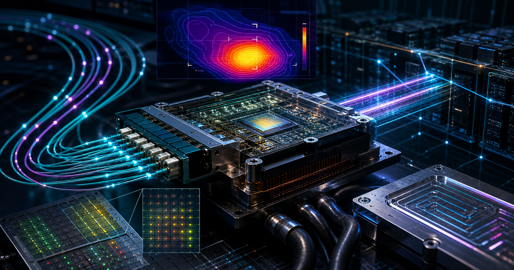
私はもともとEEPROMの車載プロセス開発をしていた人間で、メモリ素子の挙動を TCAD で何百回も叩いてきました。だから2026年5月14日に日経が報じた東大の「不揮発量子スイッチング素子」——タンタル + マンガンスズで動き、1ビット 40ピコ秒、しかも発熱がほぼ出ないという素子——を見た瞬間、頭の中で2つの感情が同時に走りました。「これは本物の物理だ」というワクワクと、「2030年実用試作と言われると投資家としては微妙な距離」という現場感です。今回はこの素子を、投資テーマとして冷静に分解します。
最初に、報道の数字を投資家目線で並べ直しておきます。
| 指標 | 値 | 既存比較 | 含意 |
|---|
| ビット切替時間 | 40ピコ秒 | 従来素子比 約1/1000 | 演算スループットの素子側上限を上方向にずらせる |
| 動作機構 | スピン(電子磁化)切替 | 電流ベースのトランジスタと別系統 | ジュール熱の主要発生源を回避できる |
| 耐久性 | 1000億回以上で安定 | DRAM並み〜以上 | 揮発・不揮発両用途を見据えやすい |
| 構成素材 | タンタル + マンガンスズ | レアアース不要・既存ファブ素材 | サプライチェーン拘束は比較的軽い |
| 実用試作目標 | 2030年 | — | 量産は2030年代後半以降が現実線 |
私の目には、最大の価値は速度より「発熱が出にくい」側にあります。AIデータセンターのTCOは、いまや演算コストより冷却・電力コストが律速になりつつある。Nvidia GB200ラックの消費電力は120kW級で、データセンター側の電気・水・空調投資が追いつかない。素子レベルで発熱を引き下げられること自体が、AIインフラ投資の制約を1段階ずらすイベントになり得ます。
速さは結局「動かせる枚数」の話。発熱は「動かし続けられる総量」の話。投資テーマとしては後者の方が市場規模が大きい——これが私の現時点の見立てです。
報道だけ追うと「またMRAMか」と感じる読者もいると思うので、ここはきちんと書きます。
| 方式 | 切替原理 | 切替速度の目安 | 耐久 | 量産現況 |
|---|
| STT-MRAM | スピン注入トルク | ナノ秒〜数百ピコ秒 | 10^12回前後 | Everspin、Samsung(一部eMRAM)が量産中 |
| SOT-MRAM | スピン軌道トルク | 100ピコ秒前後 | 10^14回級 | TSMC、Intelが研究レベルで量産前夜 |
| 東大 不揮発量子スイッチング | 量子状態の切替 | 40ピコ秒 | 10^11回以上で安定確認 | 試作段階・2030年に量産前試作目標 |
数字だけ見ると「SOT-MRAMをさらに高速化した上位互換」に見えるが、私はそう単純化したくない。SOT-MRAMはCMOSプロセスとの相性が既に良く、量産前夜の段階に入っているのに対して、東大素子は素材組み合わせ(タンタル + マンガンスズ)の堆積プロセスと既存300mmラインとの整合性が、今後の最大の関門になります。半導体は「物理が正しい」ことと「量産できる」ことの間に、毎回ファブ5〜10年分の溝が横たわります。
私は車載 EEPROM の量産化を現場で経験しましたが、研究段階の「動きました」と量産段階の「歩留まり90%以上で動き続けます」の間には、CDコントロール・パーティクル管理・装置の前後相関——目に見えない要素の塊があった。新素子のニュースを見るたびに、私が真っ先に頭をよぎるのはここです。
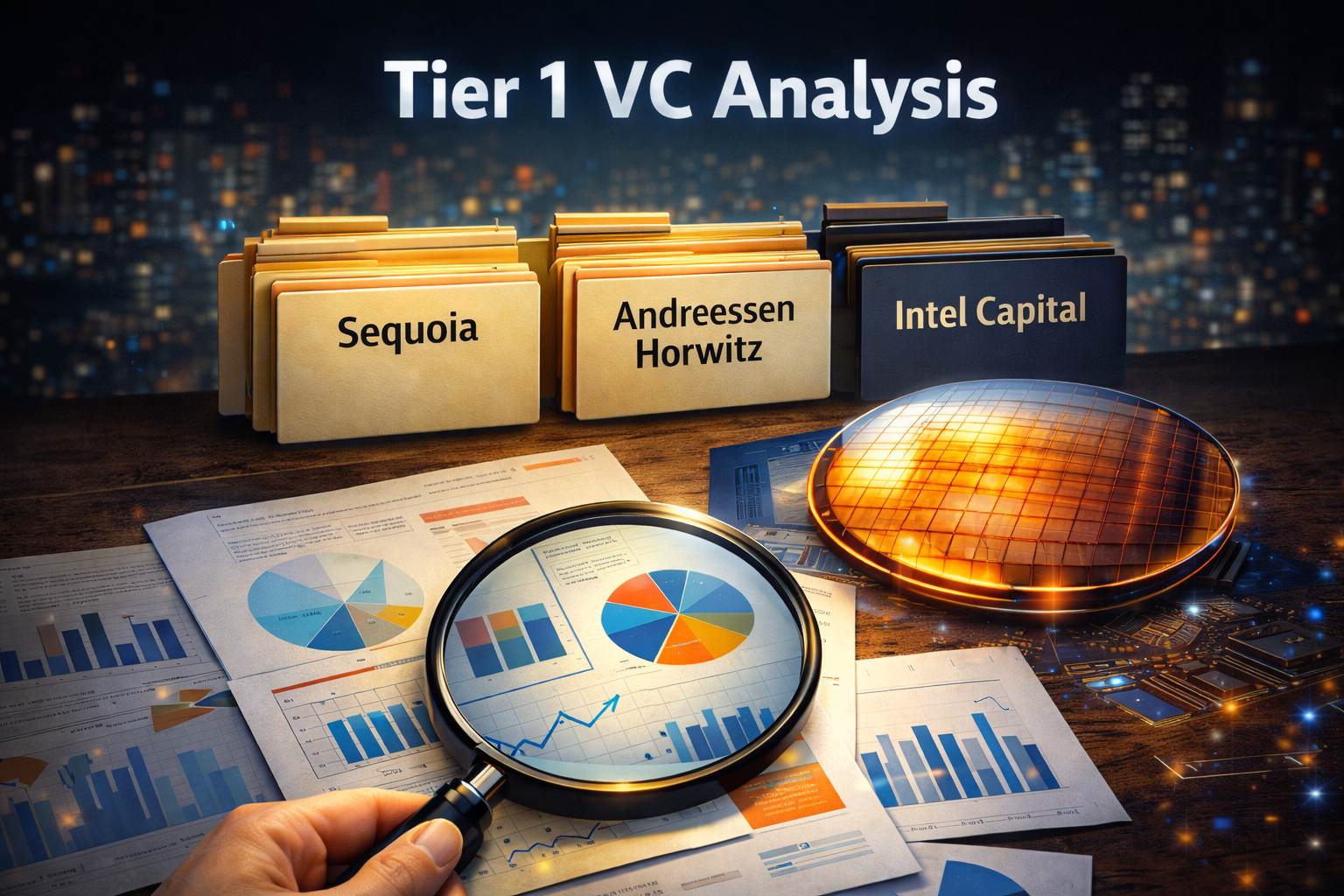
ZYL0で半導体テーマを書くときは、いつも直接受益/間接受益/二次波及の3階層に分けます。今回も同じ枠で整理しておきます。
| カテゴリ | 銘柄候補 | ロジック |
|---|
| 高純度金属(タンタル/マンガン系) | JX金属(5016 JP)、住友化学(4005 JP)、信越化学(4063 JP) | 新素子の組成側で「材料純度・成膜均一性」がボトルネックになる |
| 成膜・スパッタ装置 | アルバック(6728 JP)、東京エレクトロン(8035 JP)、Applied Materials(AMAT) | スピン素子は積層均一性が命。PVD/ALDの技術差分が露出 |
| 計測・検査 | KLA Corp(KLAC)、レーザーテック(6920 JP) | 新素子は素子間バラつき検査の難度が一段上がる |
| パワー周辺 | ロームのパワー半導体、SCSK のEDA関連、Cadence/Synopsys | 低発熱素子をシステムに織り込む電源/設計サイドの恩恵 |
このカテゴリの特徴は、「素子が量産化できなくても、研究開発投資自体が需要を作る」ことです。2026〜2029年は量産前の試作・装置投資のフェーズなので、装置・素材は研究開発支出側からの需要が先行します。
| 銘柄 | ポジション | コメント |
|---|
| TDK(6762 JP) | HDD磁気ヘッド由来のスピン技術蓄積 | スピン技術の特許・人材プールで間接的に潤いやすい |
| 村田製作所(6981 JP) | センサー・コンデンサ経由のスピン関連IP | 量産品でなく研究側でアセットが効くタイプ |
| Western Digital(WDC) | スピントロニクス系の長期R&D継続 | 米側のスピン特許とライセンス交渉力 |
ここは「直接の売上貢献」というより、特許プールと人材の希少性プレミアムで評価される領域。CVCの目線で言うと、買収やジョイントベンチャー時に表に出てくる類の資産です。
ここが本記事の本丸です。素子の速度や発熱が1〜2桁改善されたとき、何の制約が外れるかを考えます。
| 制約が外れる領域 | 想定アプリ | 主な受益候補 |
|---|
| エッジAI推論 | スマホ・XRデバイス・産業センサー上で大規模モデルが動く | Apple(AAPL)、Qualcomm(QCOM)、Arm(ARM) |
| フィジカルAI / ロボティクス | ロボットのオンボード推論で熱・電力制約緩和 | Nvidia(NVDA)、Boston Dynamics親、ファナック(6954 JP)、安川電機(6506 JP) |
| 衛星・宇宙機 | 宇宙環境での放射線耐性 × 低消費電力 | Rocket Lab(RKLB)、三菱重工(7011 JP)の宇宙系 |
| データセンター冷却需要の頭打ち | 1ラックあたりの計算密度がもう一段上がる | Vertiv(VRT)、SuperMicro(SMCI)、Eaton(ETN) |
低発熱の素子は「データセンター内」より「データセンターの外」で投資価値が大きい、と私は見ています。なぜなら、データセンターの中での発熱は冷却投資(液冷・浸漬冷却)で吸収できるが、スマホやロボットの中では物理的に冷却装置を置けないからです。フィジカルAIの時代に「電池1個で動くAGI級モデル」を成立させる素子は、最大の市場が外側にあります。
新素子の話で最も誤解されやすいのが時間軸です。投資家向けに、私の現時点の見立てを表にします。
| 期間 | 段階 | 投資家の主要アクション |
|---|
| 2026〜2028 | 基礎研究・追試・特許戦 | 直接受益(装置・素材)に薄く広く。個別新素子ベットは時期尚早 |
| 2028〜2030 | 量産前試作・大手参入 | Intel/Samsung/TSMCのR&D開示を毎四半期チェック。装置受注の見える化 |
| 2030〜2033 | 量産前夜・パイロット量産 | スピン技術IP保有銘柄が買収・ライセンス交渉で動く局面。M&A銘柄を組み込む |
| 2033〜2035 | 限定量産・特定用途搭載 | 二次波及(フィジカルAI、エッジAI、宇宙)が本格化。最大の収益貢献はここから |
| 2035〜 | 主流化シナリオ if 量産 OK | NAND/DRAMサイクルへの構造的影響。Intel/Micron/Samsungの設備配分が変わる |
私の中の経験則として、「Science誌掲載・大学発・量産試作は5年後」と言われた素子が、5年後に量産に到達した確率は体感で2〜3割です。物理として正しくても、装置・歩留まり・コストの三重壁を全部抜けるのは難しい。だから現時点では、「素子そのもの」を本命視するより「素子開発が活発化する局面の周辺需要」を取る方が、ペイオフ × 確率で見て優位だと考えています。
最後に、自分が投資委員会に出すならどう書くか、というつもりで3シナリオを置きます。
| シナリオ | 中身 | 確率(私の主観) | 主な受益 |
|---|
| ベース | 2030年に試作チップ、2033年に限定量産。エッジAI・宇宙機で特化採用 | 50% | 装置・素材、TDK等のIP保有、Apple/Qualcomm |
| 強気 | 2032年に主流ロジック/メモリ階層に組込み、Intel/Samsungが大規模採用 | 20% | Intel・Samsung・Micron・東京エレクトロン・Applied Materials |
| 弱気 | 量産プロセス互換が達成できず、競合(SOT-MRAM等)に置き換わる | 30% | 既存スピントロニクスの量産勝者(TSMC・Everspin)が結局取る |
落とし穴は3つ。(1) スケーリング限界——研究室の単素子が動いても、ナノスケール集積で揃って動くかは別問題。(2) 製造プロセス互換性——タンタル/マンガンスズ系の堆積プロセスが既存CMOSラインで「汚染」とみなされないかは、装置メーカー側の対応力に左右されます。(3) 競合の追随——Intel・Samsung・IBM 等は独自スピン素子を長年抱えている。「東大が世界初」ではなく「東大が今回いい結果を出した」という温度感で見るのが正確です。
CVCとして投資委員会で扱うなら、私は「素子ベットではなく装置・素材・IP保有銘柄でテーマを取る/スタートアップは2028〜2030に量産前夜で再評価」という指針を置きます。これは、半固体電池のときに私自身が現場で取ったポジショニング——技術が正しくても量産前のスタートアップに早く張りすぎるとIRRが死ぬ——と同じロジックです。
note でこの素子を紹介していた reika1021 さんの記事タイトルが「東大の新素子は半導体の常識を壊すのか?」だったのが象徴的で、答えは私の見立てでは「常識は変えるが、変わるのは2030年代後半。今は受益する周辺をきちんと取りに行く時期」です。
- 案1:数字で追う続編 — 本記事の前提を最新データで更新し、何が強まり、何が崩れたかを再点検する。
- 案2:実務テンプレート編 — 読者が自分の投資判断、制作単価、または開発運用に転用できるチェックリストへ落とし込む。
- 案3:反対シナリオの検証 — 今回の見立てが外れる条件を先に定義し、次に見るべき指標と時間軸を整理する。
本文の事実関係と数値前提は、再審査時にも読者が確認できる一次情報・公的資料を優先して見直しています。
本記事は情報提供を目的としたものであり、特定の銘柄、サービス、契約条件の推奨や投資助言ではありません。執筆者は記事内で触れた銘柄やサービスにポジションまたは利害関係を持つ可能性があります。調査、翻訳、校正の一部に生成AIを利用していますが、最終的な内容はZYL0が確認しています。詳細は免責事項をご確認ください。
Will the University of Tokyo's Nonvolatile Quantum Switching Element Rewrite Semiconductor Investing? Key Names and the Timeline
I started my career as an in-line process engineer building automotive EEPROM, slamming TCAD against memory device behavior hundreds of times. So when Nikkei reported on May 14, 2026 about the University of Tokyo team's "nonvolatile quantum switching element" — built from tantalum and manganese-tin, switching a bit in 40 picoseconds, and emitting almost no heat — two things hit me at once. First, "that's real physics." Second, "2030 prototype" is exactly the awkward distance for an investor. Below I break it down as an investment theme, cold-eyed.
Let me re-table the headline numbers from the investor's seat.
| Metric | Value | Comparison | Implication |
|---|
| Bit switching time | 40 picoseconds | ~1/1000 of conventional | Lifts the device-side ceiling on compute throughput |
| Mechanism | Spin (electron magnetization) flip | Different family from current-driven transistors | Sidesteps the dominant source of Joule heat |
| Endurance | Stable >100 billion cycles | Comparable to or beyond DRAM | Plausible for both volatile and nonvolatile roles |
| Materials | Tantalum + manganese-tin | No rare earths, existing fab materials | Supply-chain lock-in is relatively mild |
| Prototype target | 2030 | — | Mass production realistically late 2030s |
In my eyes, the bigger prize is on the heat side rather than the speed side. AI data-center TCO is increasingly rate-limited by cooling and power, not compute. A single Nvidia GB200 rack draws ~120 kW, and utility and HVAC capex can't keep up. A device-level cut in heat generation is exactly the kind of event that loosens an entire AI-infrastructure constraint by one notch.
Speed is a story about "how many chips you can run." Heat is a story about "how long you can keep running them." The latter is the larger investable market — that's my current read.
A fair reader will ask "another MRAM?" I want to handle that carefully.
| Approach | Switching mechanism | Switching speed | Endurance | Production status |
|---|
| STT-MRAM | Spin-transfer torque | ns to several hundred ps | ~10^12 cycles | Everspin, Samsung (partial eMRAM) in production |
| SOT-MRAM | Spin-orbit torque | ~100 ps | ~10^14 cycles | TSMC, Intel at research / pre-production |
| UTokyo nonvolatile quantum element | Quantum-state switching | 40 ps | >10^11 confirmed | Prototype, 2030 pre-mass-production target |
On paper this looks like "a faster SOT-MRAM." I don't want to over-simplify it. SOT-MRAM already has good CMOS process compatibility and sits at pre-production, while for the UTokyo element, the integration of a tantalum / manganese-tin stack with existing 300 mm lines is the gating risk going forward. In semiconductors, the gap between "physics works" and "yields above 90%" is always five to ten fab-years wide.
I lived this in EEPROM volume production: between a research "it switches" and a production "it switches at high yield, forever" there is a mountain of invisible inputs — CD control, particle management, tool-to-tool correlation. Every time a new-device headline lands, that mountain is the first thing I see.
When I write semi themes on ZYL0 I always split them into direct / indirect / second-order beneficiaries. Same frame here.
| Category | Candidates | Logic |
|---|
| High-purity metals (Ta / Mn-based) | JX Metals (5016 JP), Sumitomo Chemical (4005 JP), Shin-Etsu Chemical (4063 JP) | Purity and film-uniformity become the bottleneck on the materials side |
| Deposition / sputter equipment | ULVAC (6728 JP), Tokyo Electron (8035 JP), Applied Materials (AMAT) | Spin devices live or die on stack uniformity; PVD/ALD differentiation surfaces |
| Metrology / inspection | KLA Corp (KLAC), Lasertec (6920 JP) | Inter-device variation inspection becomes one step harder |
| Power / EDA periphery | ROHM power semis, Cadence/Synopsys (EDA) | Designing low-heat devices into systems benefits the power/design side |
What's nice about this layer is that R&D spending creates demand even before any element reaches mass production. The 2026–2029 window is the pre-production prototype and capex phase, so equipment and materials see demand from R&D budgets first.
| Name | Position | Comment |
|---|
| TDK (6762 JP) | Deep spintronics legacy from HDD magnetic heads | Patents and talent pool likely to monetize through licensing |
| Murata (6981 JP) | Spin-related IP via sensors and components | Asset-side, not P&L-side, leverage |
| Western Digital (WDC) | Sustained long-term spintronics R&D | US-side patents and licensing leverage |
This layer is priced on patent-pool and talent-scarcity premia rather than direct revenue. From a CVC seat, this is the kind of asset that surfaces in M&A and JV negotiations.
This is the heart of the post. What is unlocked once device speed and heat improve by one to two orders of magnitude?
| Constraint relaxed | Application | Likely beneficiaries |
|---|
| Edge AI inference | Running larger models on phones, XR devices, industrial sensors | Apple (AAPL), Qualcomm (QCOM), Arm (ARM) |
| Physical AI / robotics | On-board inference under thermal/power budgets | Nvidia (NVDA), Boston Dynamics' parent, Fanuc (6954 JP), Yaskawa (6506 JP) |
| Satellites / spacecraft | Radiation tolerance × ultra-low power | Rocket Lab (RKLB), Mitsubishi Heavy Industries (7011 JP) space arm |
| Saturation of data-center cooling | Another step-up in per-rack compute density | Vertiv (VRT), Super Micro (SMCI), Eaton (ETN) |
Low-heat devices, in my view, create more value outside the data center than inside it. Inside the data center, heat can be absorbed by liquid and immersion cooling. Inside a phone or a robot, you physically cannot bolt on a cooling rig. The era of physical AI needs devices that allow AGI-class inference on a single battery, and most of that market lives outside the rack.
The most common error on new-device stories is the timeline. Here is my current view, framed for investors.
| Window | Stage | Investor action |
|---|
| 2026–2028 | Basic research, replication, patent jockeying | Thin, broad exposure to equipment/materials. Single-device bets are premature. |
| 2028–2030 | Pre-production prototyping, hyperscaler R&D entry | Track Intel/Samsung/TSMC R&D disclosures quarterly. Look for equipment orders. |
| 2030–2033 | Late-stage R&D, pilot production | Spin IP holders start moving on M&A / licensing. Add positions in those names. |
| 2033–2035 | Limited mass production, specialty integration | Second-order plays (physical AI, edge AI, space) start producing revenue |
| 2035– | Mainstream scenario (if production sticks) | Structural disruption to the NAND/DRAM cycle; Intel/Micron/Samsung capex mix shifts |
My personal rule of thumb: "Science-published, university-led, mass production in five years" elements actually reach mass production roughly 20–30% of the time. Right physics still has to clear the triple wall of tooling, yield, and cost. So for now, picking the surrounding demand around active device R&D pays off better — on a payoff × probability basis — than picking the device itself.
To close, I'll write the way I would for an investment committee — three scenarios.
| Scenario | Storyline | Subjective probability | Main beneficiaries |
|---|
| Base | Prototype chip in 2030, limited production in 2033, niche edge/space adoption | 50% | Equipment & materials, IP holders such as TDK, Apple/Qualcomm |
| Bull | Mainstream logic/memory integration by 2032, large-scale Intel/Samsung adoption | 20% | Intel, Samsung, Micron, Tokyo Electron, Applied Materials |
| Bear | Process compatibility never lands; SOT-MRAM and rivals eat the niche | 30% | Mass-production winners in existing spintronics (TSMC, Everspin) |
Three pitfalls. (1) Scaling limits — a single device that works in the lab is a different problem from a nanoscale array that switches in unison. (2) Process compatibility — whether a Ta / Mn-Sn stack avoids being treated as contamination in a standard CMOS line depends heavily on the toolmakers. (3) Incumbent response — Intel, Samsung, IBM have been running their own spin devices for years; this is "UTokyo printed a strong result," not "UTokyo invented spintronics."
If I were writing the IC memo, my guidance would be: avoid betting the device itself; take the theme through equipment, materials, and IP holders; re-evaluate startups in 2028–2030 at pre-production. It is the same playbook I used in semi-solid batteries — physics can be right and IRR can still die if you go in too early before mass production.
Reika1021's note.com post titled "Will the UTokyo new element break the semiconductor canon?" captures the mood well. My answer is: yes, the canon will change — but the change lands in the late 2030s. For now, take the periphery that benefits from active research, cleanly.
- Idea 1: A data-updated follow-up — Revisit the thesis with fresh numbers and separate what strengthened from what broke.
- Idea 2: A practical template edition — Turn the article into a checklist readers can reuse for investing, pricing, or technical operations.
- Idea 3: The bear-case test — Define the conditions that would invalidate this view and map the indicators to watch next.
The factual and numerical assumptions in this article are anchored to primary or public materials that readers can revisit during AdSense review and future updates.
This article is for informational purposes only and does not constitute investment advice or a recommendation of any specific stock, service, or contract structure. The author may hold positions or interests related to companies or services mentioned. Generative AI was used for parts of research, translation, and proofreading, with final review by ZYL0. See the disclaimer for details.