スピントロニクス投資ロードマップ2030|東大新素子の前に買われる装置・素材・IP
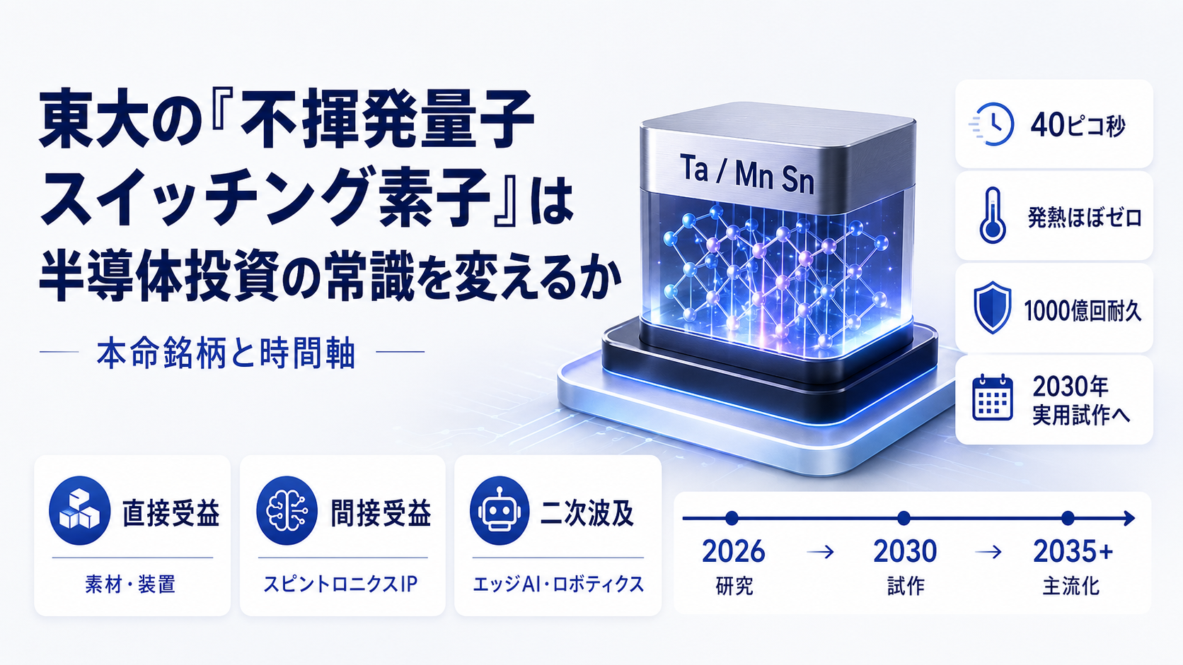
前回、東大の不揮発量子スイッチング素子を「2030年代後半に常識を変え得るが、今すぐ素子ベットする段階ではない」と書きました。今回はその続編として、もう一段実務寄りに落とします。素子の物理と本命銘柄、時間軸の全体像はデバイス解説編の別記事にまとめています。では投資家は、量産まで待つしかないのか。 私の答えは違います。
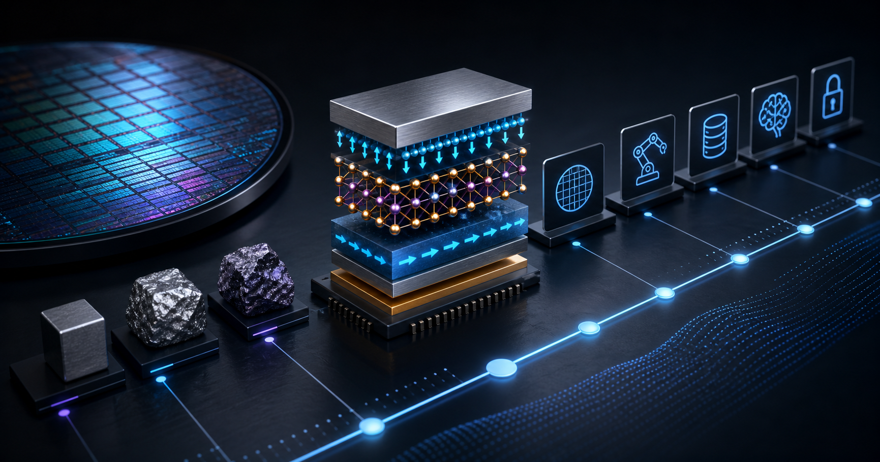
半導体の新素子テーマでは、素子そのものより先に、装置・材料・検査・IP・人材の価格が動きます。私がEEPROMの量産プロセスで学んだのは、「動く素子」より「再現よく作れる工程」の方が、はるかに早くお金になるということでした。東大の40ピコ秒スイッチングも、投資テーマとしては同じ読み方をした方がよいと見ています。
新素子の報道を見ると、どうしても本命デバイスを探したくなります。ただ、2026年時点で一番確度が高いのは、量産収益ではなく研究開発の増加です。
| レイヤー | 2026〜2030年に増えるもの | 投資家が見るべき変化 |
|---|
| 素材 | Mn3Sn、Ta、重金属膜、高純度ターゲット | 研究向けから量産品質へ要求が上がる |
| 成膜装置 | PVD、ALD、スパッタ、アニール | 膜厚均一性と界面制御の要求が厳しくなる |
| 検査 | 磁気特性、ナノスケール膜厚、欠陥検査 | KLA/レーザーテック型の検査需要が先に立つ |
| EDA/IP | MRAMマクロ、低消費電力設計、熱設計 | 既存SoCへの統合検討が始まる |
| 人材 | 磁性材料、スピン輸送、CMOS統合 | 大手半導体の採用・買収が始まる |
ここで大切なのは、売上が出る順番です。素子メーカーの量産売上はまだ遠い。しかし装置・材料・検査は、試作ラインが増えるだけで売上が立ちます。私には、2026〜2030年は「新素子の勝者を当てる時間」ではなく、「試作が増える周辺を拾う時間」に見えます。

スピントロニクス投資で危ないのは、全部を「次世代MRAM」とまとめてしまうことです。技術の位置が違えば、投資時間軸も違います。
| 技術 | 現在地 | 投資時間軸 | 見るべき勝ち筋 |
|---|
| STT-MRAM | すでに一部量産 | 2026〜2028 | 既存組込み用途、車載・産業向け採用 |
| SOT-MRAM | 量産前夜〜研究 | 2027〜2032 | 高速・高耐久メモリ、ファウンドリ統合 |
| 反強磁性スピントロニクス | 研究・試作 | 2028〜2035 | 超高速・低発熱、光/電気パルス統合 |
| 東大系量子スイッチング | 基礎実証 | 2030〜2038 | AI/エッジ/宇宙向けの特殊用途から開始 |
STT-MRAMは「もう動いている市場」、SOT-MRAMは「ファウンドリが本気になるかを見る市場」、反強磁性スピントロニクスは「研究費とIPが動く市場」です。東大の成果は最後のレイヤーに近い。だから、短期投資ではSTT/SOTの既存プレイヤーを無視せず、中期テーマとして反強磁性材料・装置・検査を重ねる方が現実的です。
半導体プロセスの現場にいた感覚で言うと、材料が変わるテーマは毎回、界面でつまずきます。膜は堆積できる。単素子も動く。けれど量産では、ウェハ面内ばらつき、熱処理、汚染管理、装置間差が一気に効いてくる。ここを突破する企業が、本当の意味でテーマを取ります。
個別銘柄を一発で当てるより、レイヤーごとにかごを分ける方が、このテーマには向いています。
| かご | 候補例 | 期待するドライバー | 主なリスク |
|---|
| 素材 | JX金属、住友化学、信越化学 | 高純度金属、特殊ターゲット、材料評価 | 研究需要止まりで量産規模にならない |
| 装置 | 東京エレクトロン、ULVAC、Applied Materials | 成膜・アニール・エッチング工程の高度化 | 既存装置の延長で差別化が薄い |
| 検査 | KLA、レーザーテック、HORIBA | 欠陥・膜厚・磁気特性の計測需要 | 顧客側の開発予算縮小 |
| IP/統合 | TDK、Western Digital、Cadence、Synopsys | スピン系IP、EDA、SoC統合 | 収益化まで時間がかかる |
私がポートフォリオを組むなら、短期は検査と装置を厚めにします。理由は単純で、研究開発が増えるだけで受注につながりやすいからです。素材は量産採用が見えると強いが、試作用の売上だけでは大型テーマになりにくい。IPは一番面白い反面、買収・ライセンス・標準化のタイミングが読みにくい。
このあたりは半固体電池の投資でも似ていました。セルそのものの勝者を早く当てようとすると、量産の遅れでIRRが苦しくなる。一方、評価装置、材料、量産技術、顧客実証の周辺は先に動く。スピントロニクスも、私は同じ構造で見ています。
CVC目線では、スピントロニクス系スタートアップはまだ数が多くありません。だからこそ、来た案件を「面白い物理」だけで評価すると危ない。私なら、最低限この3条件を置きます。
- CMOS互換の工程説明がある
300mmラインで何が汚染源になり、どの装置で回避するのかを説明できるか。 - 単素子ではなくアレイのデータがある
1ビットが動くことより、ばらつき込みで複数セルが揃って動くことが重要。 - 用途をメモリだけに閉じていない
エッジAI、センサー、宇宙、低発熱ロジック補助など、最初の小さい市場を持っているか。
特に3つ目は大事です。新メモリがDRAMやNANDをいきなり置き換える、という話は投資委員会では通りにくい。むしろ「宇宙機の低消費電力不揮発メモリ」「産業センサーのエッジ推論」「ロボット内の熱制約付きAI」など、小さいが切実な用途から入る方が現実的です。
最後に、時間軸を置きます。私ならこのテーマを、以下のように段階管理します。
| 時期 | 技術イベント | 投資アクション |
|---|
| 2026〜2027 | 大学・研究機関の追試、特許出願増加 | 装置・検査を薄く拾う。素子ベットはまだ控えめ |
| 2028〜2030 | 大手半導体・ファウンドリの共同研究増加 | 素材・IPを追加。スタートアップDDを開始 |
| 2030〜2032 | 試作チップ、限定用途デモ | 買収候補・ライセンス保有企業を重視 |
| 2033〜2035 | 特殊用途で限定量産 | エッジAI、宇宙、ロボティクス側の二次波及を取る |
| 2035以降 | 主流メモリ/ロジック統合の可能性 | 量産勝者に集中。ただし敗者も多い |
結論はかなり地味です。2026年時点のスピントロニクス投資は、夢を見るテーマではなく、研究開発の増加を周辺レイヤーで取るテーマだと私は考えています。東大の成果は、その物語を一段進めました。ただし、収益が先に立つ場所は、素子そのものではなく「作る・測る・統合する」企業です。
次に見るべきニュースは、大学発表よりも、大手ファウンドリの共同研究、装置メーカーのR&D顧客、そしてスピン系IPの買収です。そこに資金が流れ始めたら、このテーマは研究ニュースから投資テーマに変わります。
- MRAM量産プレイヤー比較|Everspin、Samsung、TSMC、Intelの現実線:STT/SOT-MRAMの量産状況と、どこが最初に利益化するかを整理。
- 低発熱半導体がフィジカルAIを変える理由:データセンターより、ロボット・XR・宇宙機で価値が大きくなる仮説を深掘り。
- 大学発半導体技術をCVCがどうDDするか:論文、特許、量産工程、顧客用途をどう切り分けるかの実務編。
- 案1:数字で追う続編 — 本記事の前提を最新データで更新し、何が強まり、何が崩れたかを再点検する。
- 案2:実務テンプレート編 — 読者が自分の投資判断、制作単価、または開発運用に転用できるチェックリストへ落とし込む。
- 案3:反対シナリオの検証 — 今回の見立てが外れる条件を先に定義し、次に見るべき指標と時間軸を整理する。
本文の事実関係と数値前提は、再審査時にも読者が確認できる一次情報・公的資料を優先して見直しています。
本記事は情報提供を目的としたものであり、特定の銘柄、サービス、契約条件の推奨や投資助言ではありません。執筆者は記事内で触れた銘柄やサービスにポジションまたは利害関係を持つ可能性があります。調査、翻訳、校正の一部に生成AIを利用していますが、最終的な内容はZYL0が確認しています。詳細は免責事項をご確認ください。
Spintronics Investment Roadmap 2030: Equipment, Materials, and IP Before the UTokyo Device
In the previous article, I argued that the University of Tokyo's nonvolatile quantum switching element could change the semiconductor canon in the late 2030s, but that it is too early to make a direct device bet. This is the practical sequel. The device-side explainer — the physics, key names, and timeline — is covered in the companion post. Does that mean investors simply wait for mass production? I do not think so.
In new-device semiconductor themes, equipment, materials, inspection, IP, and talent usually reprice before the device itself generates revenue. What I learned in automotive EEPROM process engineering is that a "device that works" and a "process that repeats at yield" are two different assets. The 40-picosecond switching result should be read through the same lens.
When a new device headline lands, the temptation is to hunt for the single winner. But in 2026, the highest-confidence signal is not mass-production revenue. It is more R&D activity.
| Layer | What grows in 2026-2030 | What investors should watch |
|---|
| Materials | Mn3Sn, Ta, heavy-metal films, high-purity targets | Requirements moving from research grade to production grade |
| Deposition tools | PVD, ALD, sputtering, annealing | Tighter film uniformity and interface control |
| Inspection | Magnetic properties, nanoscale film thickness, defects | Earlier demand for KLA / Lasertec-type inspection |
| EDA / IP | MRAM macros, low-power design, thermal design | Early integration studies into existing SoCs |
| Talent | Magnetic materials, spin transport, CMOS integration | Hiring and acqui-hiring by large semiconductor firms |
The key is the order of revenue. Device revenue is distant. Equipment, materials, and inspection can generate sales as soon as prototype lines expand. To me, 2026-2030 is not the period for picking the final device winner; it is the period for owning the periphery around more experiments.
The dangerous shortcut is to label everything "next-generation MRAM." The technical position differs, so the investment timeline differs.
| Technology | Current position | Investment window | Winning path to watch |
|---|
| STT-MRAM | Partial production already | 2026-2028 | Embedded memory in automotive and industrial systems |
| SOT-MRAM | Pre-production / research | 2027-2032 | High-speed, high-endurance memory and foundry integration |
| Antiferromagnetic spintronics | Research and prototyping | 2028-2035 | Ultrafast, low-heat switching with electrical/optical pulses |
| UTokyo-style quantum switching | Basic demonstration | 2030-2038 | Special uses in AI edge, space, and thermally constrained systems |
STT-MRAM is an existing market. SOT-MRAM is a "will foundries scale it?" market. Antiferromagnetic spintronics is a research funding and IP market. The UTokyo result sits closest to that final layer. That means short-term exposure should not ignore the existing STT/SOT players, while medium-term exposure should layer in antiferromagnetic materials, tools, and inspection.
From a process-engineering seat, material changes almost always fail first at the interface. A film can be deposited. A single device can switch. Then volume production brings wafer-level variation, annealing conditions, contamination control, and tool-to-tool differences. The company that crosses that wall owns the theme.
This theme is better handled as layered exposure than as one heroic stock pick.
| Basket | Examples | Driver | Main risk |
|---|
| Materials | JX Metals, Sumitomo Chemical, Shin-Etsu Chemical | High-purity metals, special targets, material evaluation | Demand stays research-scale |
| Equipment | Tokyo Electron, ULVAC, Applied Materials | More demanding deposition, annealing, and etching | Existing tools absorb the need with little differentiation |
| Inspection | KLA, Lasertec, HORIBA | Defect, film-thickness, and magnetic-property measurement | Customer R&D budgets shrink |
| IP / integration | TDK, Western Digital, Cadence, Synopsys | Spin IP, EDA, SoC integration | Monetization takes too long |
If I were building the basket, I would overweight inspection and equipment in the early phase. The reason is simple: more R&D can become orders sooner. Materials become powerful once production adoption is visible, but prototype demand alone may not be enough. IP is the most interesting and the hardest to time, because licensing, standards, and M&A are lumpy.
This is similar to what I saw in semi-solid batteries. If you try to identify the final cell winner too early, IRR gets punished by mass-production delays. Around it, evaluation tools, materials, process know-how, and customer pilots move earlier. I read spintronics the same way.
From a CVC perspective, spintronics startups are still sparse. That makes it even more important not to fund "interesting physics" alone. I would require at least three things.
- A credible CMOS-compatibility story
Which material becomes a contamination risk on a 300 mm line, and which tool flow avoids it? - Array data, not just single-device data
One bit switching is not enough. Multiple cells need to switch with acceptable variation. - A first market outside generic memory replacement
Edge AI, sensors, space, and low-heat logic assist may be better initial targets.
The third point matters most. "This replaces DRAM or NAND" is rarely a convincing investment-committee story at the beginning. A smaller but painful market is more credible: nonvolatile low-power memory for spacecraft, edge inference in industrial sensors, or thermally constrained compute inside robots.
Here is how I would stage the theme.
| Period | Technical event | Investment action |
|---|
| 2026-2027 | Replication and more patent filings | Light exposure to equipment and inspection; avoid pure device concentration |
| 2028-2030 | More joint research with large semis and foundries | Add materials and IP; begin startup diligence |
| 2030-2032 | Prototype chips and limited-use demos | Focus on acquisition targets and license holders |
| 2033-2035 | Limited production in specialty use cases | Capture second-order exposure in edge AI, space, and robotics |
| 2035 onward | Potential mainstream memory / logic integration | Concentrate in production winners, while expecting many losers |
The conclusion is deliberately unglamorous. In 2026, spintronics investing is not about buying the dream directly. It is about capturing the R&D expansion through the layers that make, measure, and integrate the device. The UTokyo result pushes the story forward. But the first revenue will likely sit around the device, not inside it.
The next signals I would watch are not only university announcements. I would watch foundry partnerships, toolmaker R&D customers, and acquisitions of spin-related IP. Once capital starts flowing there, the theme moves from research news to investable market.
One practical way to hold this discipline is to size positions by evidence, not by excitement. Early on, when the only proof points are papers and single-device demos, the equipment and inspection baskets deserve most of the weight, because their revenue depends on the number of experiments rather than the success of any one device. As array-level yield data, foundry pilot lines, and the first licensing deals appear, capital can rotate toward materials, IP holders, and eventually the production winners. The mistake I most want to avoid is the opposite path — concentrating in a single pre-production startup on the strength of a beautiful physics result, then watching the internal rate of return decay while the process wall gets crossed years later than promised. Spintronics rewards patience precisely because the science is real; the returns simply arrive first in the companies that make, measure, and integrate the device, not in the device itself.
- Comparing MRAM production players: Everspin, Samsung, TSMC, and Intel — where STT/SOT-MRAM is actually commercializing.
- Why low-heat semiconductors matter more for physical AI than data centers — the edge, robotics, XR, and space angle.
- How a CVC diligences university-originated semiconductor technology — papers, patents, process flow, and first customer markets.
The factual and numerical assumptions in this article are anchored to primary or public materials that readers can revisit during AdSense review and future updates.
This article is for informational purposes only and does not constitute investment advice or a recommendation of any specific stock, service, or contract structure. The author may hold positions or interests related to companies or services mentioned. Generative AI was used for parts of research, translation, and proofreading, with final review by ZYL0. See the disclaimer for details.