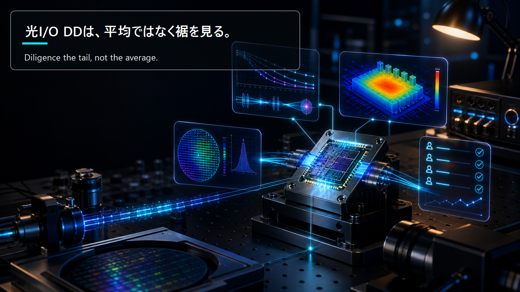
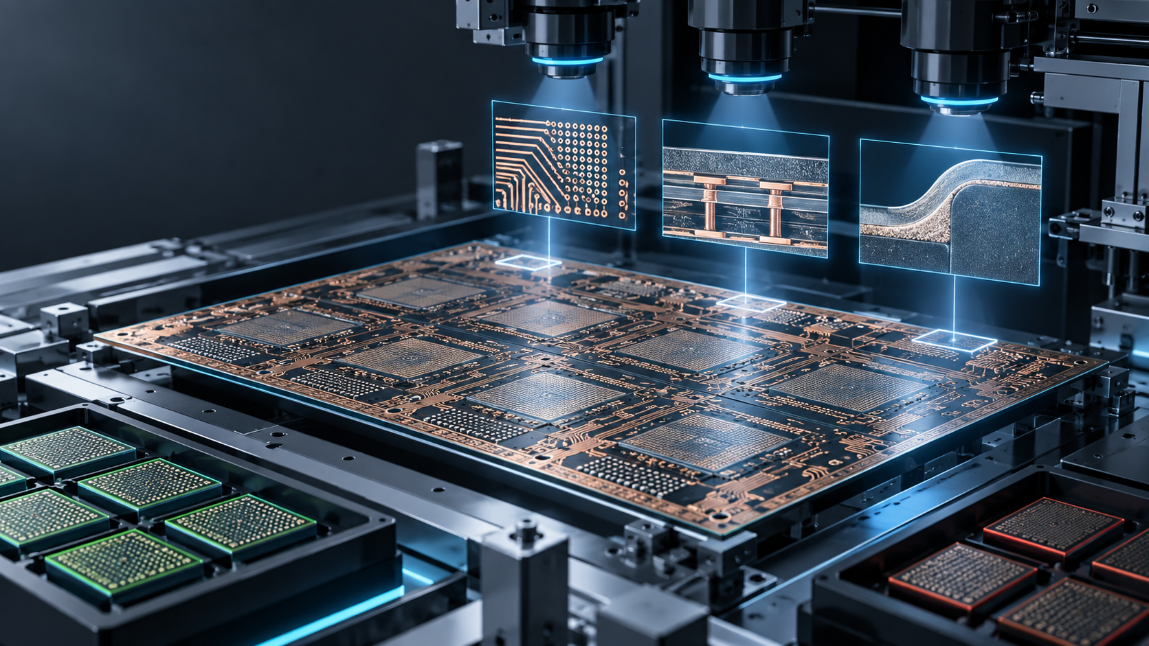
光I/Oスタートアップの見方|挿入損失・熱・量産・顧客評価を公開情報からどう読むか
前回(LPO vs CPO 移行マップ)の末尾で、次号案2として「光I/Oスタートアップの見方」を挙げました。今回はその約束を回収します。前々回のCPO量産のリアルで「CPOの本丸は歩留まりと熱だ」と書き、移行マップで「CPOサブアセンブリとPICファウンドリで中期ポジションを作る」と結論づけました。では、その領域のスタートアップを外から見るとき、公開されている情報のうち何を、どの順番で、どんな数字で読めばいいのか——本稿はそのチェックリストです。
※本稿は各社の公開情報(発表資料・製品ページ・論文・報道)をもとにした、外部からの個人的な見立てです。
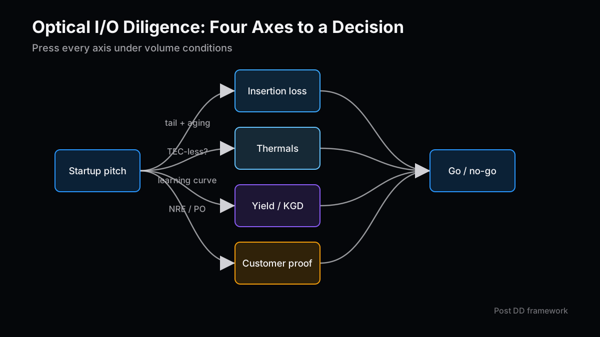
私は半導体プロセス出身でEEPROMの車載量産に関わり、TCADで「装置の問題」と報告された歩留まり不良の真因を特定した経験があります。その後CVCに移り、投資チームに投資検討の品質基準が統一されていなかった問題を見つけて標準化しました。光I/Oは「光通信銘柄」に見えますが、私の目には先端パッケージ・熱・検査の複合問題です。発表資料の綺麗なグラフに惑わされず、挿入損失・熱・量産・顧客評価の4軸を、量産条件で読む。これが本稿の主張です。あくまで2026年5月時点の見立てで、数字は半年で動きます。
最初に所感を述べると、光I/Oの発表は技術的に正しくても投資的に間違っていることがよくあります。理由は単純で、公表される数字はベスト品の研究室条件で、私が知りたいのは量産分布の裾だからです。
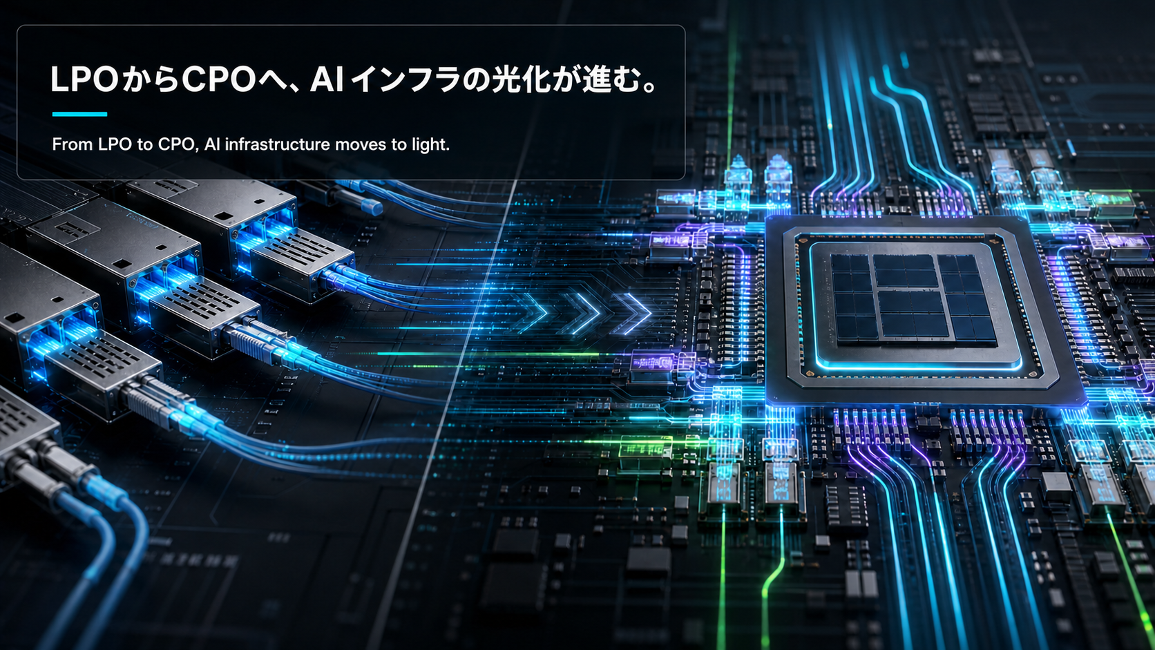
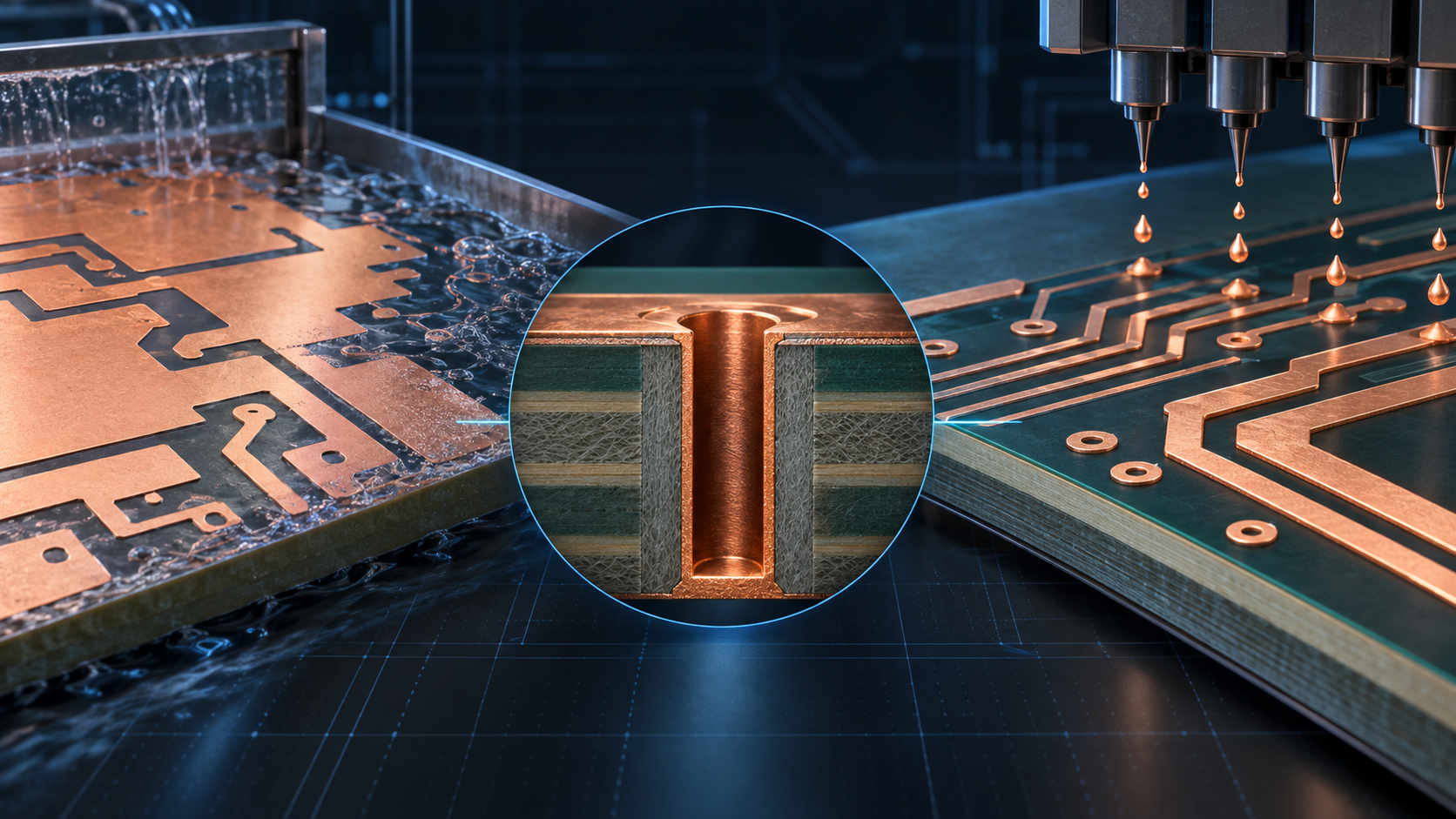
光I/Oスタートアップは大きく2系統に分かれます。CPOサブアセンブリ(光エンジン、外部レーザー、ファイバーアタッチを組む実装屋)と、PICファウンドリ/光I/O IPを持つアーキテクチャ系(Ayar Labs、Lightmatter、Celestial AI など)です。同じ「光I/O」でも、見るべき急所が違います。
| 系統 | 代表的な民間プレイヤー | 価値の源泉 | 見るべき急所 |
|---|
| CPOサブアセンブリ | 非上場実装系、Coherent/Lumentumの周辺サプライヤー | 実装・アライメント・歩留まり | 量産歩留まりとテスト能力 |
| PICファウンドリ系 | GF Fotonix、TSMC COUPE、Tower(製造)+ 非上場 | プロセスとキャパシティ | 移管性とPDKの成熟度 |
| 光I/O IP・アーキテクチャ | Ayar Labs、Lightmatter、Celestial AI | アーキテクチャと顧客design-in | 顧客評価と量産移管 |
ここで陥りやすい失敗は、技術面の評価と量産面の評価を混同することです。技術面の評価は「動くか」を見る。量産面の評価は「歩留まりと熱とコストで成立するか」を見る。光I/Oは前者で合格しても後者で落ちるケースが圧倒的に多い。本稿は後者に寄せて書きます。
評価の全体像を、測る指標・測り方・合格ラインで一枚にすると下表になります。以降の章で1軸ずつ掘ります。
| 評価軸 | 主要指標 | どう測るか | 2026年の目安ライン |
|---|
| 挿入損失 | 結合損失(dB/接続)、リンクバジェット余裕 | 量産ロットの分布、最悪値、経時劣化 | グレーティング結合 < 2dB、エッジ結合 < 1.5dB、3σで管理 |
| 熱 | 波長ドリフト(pm/℃)、TECなしマージン | 温度サイクル試験、ASIC近傍の実温度 | 動作80〜90℃で波長制御が破綻しないこと |
| 量産・歩留まり | エンジン歩留まり、KGD、テスト網羅率 | ロット間ばらつき、歩留まりラーニング曲線 | エンジン歩留まり > 60〜70%、四半期で改善傾向 |
| 顧客評価 | design-in数、認証段階、PO/NRE | 顧客の役職・契約形態・排他性 | 第三者ハイパースケーラーの評価ボードに載っているか |
光I/Oの最初の関門は結合(カップリング)です。所感として、ここで公表される数字はほぼ例外なくベスト品です。私は平均ではなく、分布の裾と経時劣化が開示されているかを見ます。
挿入損失は地味ですが、リンクバジェット全体に効きます。送信パワー、結合損失、ファイバー損失、検出感度を足し引きして、最後に何dBの余裕が残るか。CPOではこの余裕が薄く、結合損失が0.5dB増えるだけで、消費電力や誤り率に跳ね返ります。前々回で「光結合ずれは挿入損失を増やし消費電力を上げる」と書いたのは、まさにここです。
| 指標 | 良い兆候 | レッドフラグ | 確認したい情報 |
|---|
| 結合損失(中央値) | グレーティング< 2dB / エッジ< 1.5dB | ベスト品しか出さない | 量産ロット全数の分布 |
| 結合損失(最悪値・3σ) | 中央値+1dB以内 | 「最悪値は把握していない」 | 歩留まり判定基準と紐づけて確認 |
| 経時劣化 | 数千時間で< 0.5dB増 | 加速試験データなし | 温湿度・通電寿命試験の生データ |
| アライメント方式 | 受動アライメント実績 | 能動アライメント前提でタクト長大 | 1ユニットあたり実装タクトと歩留まり |
| 偏波・波長依存性 | 広帯域で平坦 | 特定波長のみ最適化 | 量産波長分布での損失分布 |
私が一番警戒するのは「能動アライメント前提」の構成です。能動アライメントは精度こそ出ますが、1ユニットごとに光らせて位置を追い込むため、タクトが伸び量産でコストが暴れます。受動アライメント(機械的な突き合わせで規定精度を出す)で歩留まりが立つ会社の方が、量産では強い。EEPROM量産でも、「合わせ込み工程」が多い製品ほど歩留まりがロットで暴れました。光I/Oでも同じ構造が出ます。
もう一点。結合損失の「中央値」がいくら良くても、3σの最悪値が判定基準を超えるロットが一定割合出るなら、その分は丸ごと歩留まりロスです。平均で語る会社は、たいてい裾を管理できていない——これは私の経験則です。
二つ目の所感。光I/Oの熱は「冷やせるか」より「温度が揺れても波長を保てるか」が本質です。
CPOは発熱するスイッチASICのすぐ隣に光エンジンを置きます。シリコンフォトニクスの変調器やリング共振器は温度に敏感で、波長が温度でずれる(典型的に数十〜100pm/℃級)。ここで設計が分かれます。TEC(熱電クーラー)やヒーターで能動的に波長を張り付けるか、温度無依存に近い設計でTECなしを狙うか。TECは効くが消費電力と原価を食う。TECレスで広い温度範囲を保てる会社は、原価と信頼性の両方で効く——私はここを強く見ます。
| 熱の論点 | 何を測るか | 良い兆候 | レッドフラグ |
|---|
| 波長ドリフト | pm/℃、制御後の残留誤差 | TECレスで広温度を維持 | TEC前提で消費電力非開示 |
| 動作温度範囲 | ASIC近傍の実ケース温度 | 85〜90℃でリンク維持 | 室温データのみ |
| 熱サイクル耐性 | -40〜125℃の繰り返し後の損失増 | 数百〜千サイクルで安定 | サイクル試験が未実施 |
| レーザー熱管理 | 外部レーザーの温度安定性 | ELSFP等で熱源を分離 | 内蔵レーザーで熱結合が強い |
| 制御電力 | 波長制御に要するW/エンジン | 低TEC/ヒーター電力 | 制御電力が省電力メリットを食う |
ここで重要なのは、熱は単体スペックでなくシステムで詰める点です。前々回で「ASIC近傍の熱密度が光エンジンの安定性を落とす」と書きましたが、スタートアップが公表するのは多くが室温・単体の数字です。私が探すのは「ASICパッケージに載ったときのケース温度はいくつで、その温度で波長制御の残留誤差はいくつか」というデータです。それが出てこない会社は、システムレベルの検証がまだ公表できる段階にない可能性が高い。
外部レーザー(ELSFPのように熱源を光エンジンから物理的に分離する思想)を採るかどうかも論点です。内蔵レーザーは集積度で有利ですが、最も熱で劣化しやすいレーザーをASICの隣に置くことになる。私は外部レーザー+冗長化の設計に、長期信頼性の観点で点を入れます。
三つ目。ここが私にとって本丸です。光I/Oは「動くデモ」と「量産」の谷が深い。
CPOはパッケージ内に光エンジンを取り込むため、Known Good Die(KGD)——載せる前に良品を保証できているか——が決定的です。プラガブルなら不良モジュールを交換できますが、CPOでは不良エンジンを一つ載せた瞬間、高価なASICパッケージごと損なう。だから「載せる前にどこまで光・電気・熱を一括テストできるか」が歩留まりとコストを支配します。前々回で挙げた5不良(結合ずれ・レーザー劣化・熱ドリフト・基板反り・テスト不足)のうち、最後の「テスト不足」が量産面の評価の中心になります。
| 量産指標 | 測り方 | 良い兆候 | レッドフラグ |
|---|
| エンジン歩留まり | 直近ロットの良品率と推移 | 60〜70%超かつ四半期改善 | 単発ベストロットのみ提示 |
| KGD保証 | 載せる前の良品判定方法 | 光・電気・熱の一括ウェハ/ダイテスト | 載せた後にしか判定できない |
| テスト網羅率 | 検査する不良モードの数 | 主要5不良を網羅 | 電気のみ、光検査が手作業 |
| 歩留まりラーニング | ロット連番での改善曲線 | 学習が立ち上がっている | 横ばい・原因が「装置のせい」 |
| プロセス移管性 | ファウンドリ/PDK依存度 | 標準PDK・複数ファウンドリ可 | 単一ラインのカスタム依存 |
| バーンイン | 初期不良の除去能力 | 光・電気同時バーンイン | バーンイン未整備 |
私の経験から、最も雄弁なのは歩留まりラーニング曲線です。ロット連番に対して良品率が右肩上がりなら、原因を切り分けて潰すループが回っている。横ばいのまま原因を装置に求めている会社は危ない。私自身、EEPROMで「装置のせい」とされた歩留まり不良の真因が、実はプロセスばらつきと別工程の相互作用だったとTCADで特定したことがあります。歩留まりが説明できない会社は、まだ真因に到達していないだけのことが多い。
移管性も外せません。単一ファウンドリの単一ラインに張り付いたカスタムプロセスは、量産でキャパ制約に直撃します。前回の移行マップで「12インチPICライン供給能力が制約条件」と書いたのはこの意味です。標準PDKに乗り、GF FotonixやTSMC COUPE、Towerのような複数ファウンドリに移せる設計の方が、スケール期に有利です。
四つ目。顧客評価は最もごまかしが効く領域です。所感として、「大手と話している」は情報量ゼロに近い。私は誰と・どの段階の・どんな契約かが公表されているかまで見ます。
光I/Oは最終的にハイパースケーラーやスイッチASICベンダーの評価ボードに載らないと意味がありません。重要なのはdesign-inの段階と、それに紐づくお金の形(NRE、PO、排他性)です。MOUやLOIは、私の中ではほぼ何も保証しません。
| 顧客シグナル | 弱い | 中 | 強い |
|---|
| 接触相手 | 調達・IR窓口 | 設計エンジニア | アーキテクチャ責任者 |
| 段階 | 紹介・NDA | 評価ボード貸出 | design-in/認証進行中 |
| お金 | 無償サンプル | NRE受領 | 量産PO・前払い |
| 排他性 | なし | 優先交渉 | 期間限定の独占供給 |
| 検証主体 | スタートアップ自身 | 顧客の一部部署 | 第三者ラボ・複数顧客 |
ここで大事なのは、スタートアップの主張を顧客側の発信で裏取りすることです。顧客企業のプレスリリース、決算説明、カンファレンスでの登壇に、同じ内容が出ているかを確かめます。私はかつて投資委員会で、スタートアップ主張のdesign-in進捗が顧客側の認識とずれていた案件を、データを持って指摘しバリュエーション交渉を主導したことがあります。顧客評価は、スタートアップの言葉ではなく顧客の言葉で確認する。
認証(certification)の重さも理解しておく必要があります。光I/Oはスイッチ ASIC(Broadcom Tomahawk、NVIDIA Spectrum、Marvell Teralynx 系)との相互運用認証が命です。認証は時間がかかり、一度通ると乗り換えコストが効く。認証進行中の会社は、技術が多少粗くても堀ができ始めている——ここは加点します。
4軸を横断して、私が投資を見送る/割り引くトリガーを一枚にまとめます。単独では致命的でなくても、複数が重なると相関して効くのが光I/Oの怖さです。
| レッドフラグ | なぜ危険か | 確認したいこと |
|---|
| ベスト品の数字しか出さない | 量産分布を管理できていない兆候 | 直近3ロットの全数分布 |
| 能動アライメント+高タクト | 量産でコストと歩留まりが暴れる | 1ユニット実装タクトと歩留まり |
| TEC前提で制御電力非開示 | 省電力メリットが消える可能性 | 波長制御の消費電力(W/エンジン) |
| KGDが「載せた後しか判定不可」 | 高価なASICを巻き込む歩留まり損 | 載せる前の良品判定方法 |
| 歩留まり横ばい+「装置のせい」 | 真因に未到達 | ロット連番の歩留まり曲線 |
| 単一ファウンドリ・カスタム依存 | スケール期にキャパ制約直撃 | 標準PDKと第二ソースの有無 |
| 顧客がMOU/LOIのみ | お金が動いていない | NRE・PO・排他条件の実体 |
| 室温データのみ | システム熱検証が未了 | ASIC近傍ケース温度での残留誤差 |
私の経験則では、いちばん危ないのは「ベスト品の数字+歩留まり横ばい+顧客はMOUのみ」の三点セットです。これは技術が動いても量産と商流が立っていない典型で、追加調達のたびにバリュエーションだけが膨らむパターンに陥りやすい。逆に、「分布で語る+歩留まり右肩上がり+NRE受領」が揃っていれば、技術が多少地味でも私は前に出ます。
最後に、CPOサブアセンブリ/PICファウンドリ系の光I/Oスタートアップ投資が、2026〜2028年でどう報われるかをシナリオで置きます。前回はLPO→CPOの主役交代タイミングに焦点を当てましたが、今回は4軸で選別したポジションのリターン分布に焦点を移しています。
| シナリオ | 確率(主観) | 内容 | 4軸の選別後に受益する型 |
|---|
| ベース | 50% | CPOは1.6Tから2027年後半に本格量産、歩留まりが律速 | 量産歩留まり+KGDを実証したサブアセンブリ |
| 強気(前倒し) | 20% | ハイパースケーラーがCPOを前倒し採用 | 認証進行中+第二ソース可のPIC・IP系 |
| 弱気(遅延) | 20% | 歩留まり・熱でCPOが遅れ、LPO延命 | TECレス熱設計+検査能力を持つ会社 |
| テール(再設計) | 10% | 熱・反りで一部設計やり直し | 検査・バーンイン・移管性に強い会社 |
ベースケースでは、勝つのは「いちばん速い光」ではなく「いちばん早く量産歩留まりとKGDを実証した実装屋」です。強気ケースでは前倒しに耐えられる認証・第二ソース持ちが報われ、弱気・テールケースでは皮肉にも検査・熱・移管性という地味な能力が価値を持ちます。どのシナリオでも共通して効くのは、本稿の4軸を量産条件で読めたかどうか。シナリオに依存せず効くのは「量産面の評価の深さ」だ、というのが私の結論です。
私がいま最もミスプライスだと感じるのは、KGDとインライン光検査を量産で回せる実装系です。市場はこれを「下請けの実装屋」としか見ていませんが、CPO量産で最初に詰まるのはここで、しかも代替が効きにくい。前回挙げたリタイマーIPやファイバーコネクタと同様、地味なボトルネックが量産期に値段を持つという構造は、光I/Oを見るときにも一貫しています。
結論として。光I/Oは技術面の評価で合格しても量産面の評価で落ちる。挿入損失は裾と経時で、熱はTECの有無とシステム実温度で、量産はKGDとラーニング曲線で、顧客評価は段階と契約で読む。この4軸を量産条件で通過したと公開情報から読める会社にだけ、私は前に出ます。2026年5月時点での見立てとして、半年後に答え合わせをします。
次号の記事案
- 案1:AIデータセンター液冷の部品表|CDU、コネクタ、冷媒、センサーの投資地図 — CPOと並走して立ち上がる液冷BOMをコンポーネント別に分解する。23・26号から残してきた「冷却周辺」の続編で、光I/Oの熱の論点と地続き。
- 案2:シリコンフォトニクスIPライセンスの経済性|PICファウンドリ vs IPベンダーのバリューチェーン — Ayar Labs、Lightmatter、Celestial AI など非上場IP系の収益モデルを、上場PICファウンドリのキャパ経済性と並べて比較する。本稿の「移管性」論点の深掘り。
- 案3:CPOサブアセンブリのKGDとテスト経済性|歩留まり1%が時価総額を動かす理由 — 量産面の評価の本丸であるKGDとインライン光検査を、コスト構造とバリュエーション感応度の観点で定量化する逆張り深掘り。
本文の事実関係と数値前提は、再審査時にも読者が確認できる一次情報・公的資料を優先して見直しています。
本記事は情報提供を目的としたものであり、特定の銘柄、サービス、契約条件の推奨や投資助言ではありません。執筆者は記事内で触れた銘柄やサービスにポジションまたは利害関係を持つ可能性があります。調査、翻訳、校正の一部に生成AIを利用していますが、最終的な内容はZYL0が確認しています。詳細は免責事項をご確認ください。
How to Read Optical I/O Startups From the Outside: Insertion Loss, Thermals, Manufacturability, and Customer Validation
At the end of the previous post (the LPO vs CPO migration map), I listed "how to read optical I/O startups" as the second next-issue idea. This piece pays off that promise. In the earlier post (the real CPO ramp) I argued that the real CPO contest is yield and thermals, and in the migration map I concluded that the medium-term positions live in CPO sub-assembly and PIC foundries. So when you look at a startup in that space from the outside, which pieces of public information do you read, in what order, and with which numbers? This post is that checklist.
Note: this piece is an outside-in read based solely on public information — company releases, product pages, papers, and press coverage.
I came up through semiconductor process engineering, worked on automotive EEPROM volume production, and once used TCAD to find the real root cause of a yield failure that had been reported as "an equipment problem." Later I moved to CVC, where I found that the investment team had no unified quality bar for investment reviews and built one. Optical I/O looks like an "optical communications" theme, but to my eye it is a combined advanced-packaging, thermal, and test problem. Do not get hypnotized by the clean charts in a release — read insertion loss, thermals, manufacturability, and customer validation under volume conditions. That is the whole argument. This is a May 2026 snapshot, and the numbers will move within six months.
Let me open with an observation: optical I/O announcements are frequently technically right and investably wrong. The reason is simple. The published numbers are best-unit, lab-condition data, and what I want to know is the tail of the volume distribution.
Optical I/O startups split into two broad lineages. There are CPO sub-assembly players (the assembly shops that build optical engines, external lasers, and fiber attach) and there are architecture/PIC-foundry players — names like Ayar Labs, Lightmatter, and Celestial AI. Both call themselves "optical I/O," but the pressure points to look at differ.
| Lineage | Representative private players | Source of value | Pressure point to look at |
|---|
| CPO sub-assembly | Private assembly shops, suppliers around Coherent/Lumentum | Assembly, alignment, yield | Volume yield and test capability |
| PIC foundry | GF Fotonix, TSMC COUPE, Tower (fabs) + private | Process and capacity | Process portability and PDK maturity |
| Optical I/O IP / architecture | Ayar Labs, Lightmatter, Celestial AI | Architecture and customer design-ins | Customer validation and volume transfer |
The easy mistake is conflating the technical question with the manufacturing question. The technical question is: does it work? The manufacturing question is: does it close on yield, thermals, and cost? Optical I/O companies pass the former and fail the latter far more often than not. This post leans hard into the latter.
If I compress the whole picture into one table — the metric, how to measure it, and a 2026 pass line — it looks like this. The chapters that follow take one axis at a time.
| Evaluation axis | Key metric | How to measure | Rough 2026 pass line |
|---|
| Insertion loss | Coupling loss (dB/connection), link-budget margin | Volume-lot distribution, worst case, aging | Grating coupling < 2dB, edge coupling < 1.5dB, managed at 3σ |
| Thermals | Wavelength drift (pm/°C), TEC-less margin | Temp-cycle tests, real case temp near ASIC | Wavelength control holds at 80–90°C operation |
| Manufacturing / yield | Engine yield, KGD, test coverage | Lot-to-lot variance, yield learning curve | Engine yield > 60–70%, improving quarter over quarter |
| Customer validation | Design-in count, certification stage, PO/NRE | Customer seniority, contract form, exclusivity | On a third-party hyperscaler's eval board |
The first gate for optical I/O is coupling. My observation is that the numbers published here are, almost without exception, best units. I do not look at the average. I look for whether the tail of the distribution and the aging behavior are disclosed.
Insertion loss is unglamorous, but it drives the entire link budget. Add and subtract transmit power, coupling loss, fiber loss, and detector sensitivity, and what matters is how many dB of margin survive at the end. In CPO that margin is thin, and an extra 0.5dB of coupling loss flows straight into power consumption or bit error rate. When I wrote in the earlier post that "coupling shift raises insertion loss and raises power," this is precisely the mechanism.
| Metric | Good sign | Red flag | What I want to see |
|---|
| Coupling loss (median) | Grating < 2dB / edge < 1.5dB | Only shows best units | Full distribution across volume lots |
| Coupling loss (worst / 3σ) | Within +1dB of median | "We don't track the worst case" | Tie it to the yield acceptance criterion |
| Aging | < 0.5dB rise over thousands of hours | No accelerated-test data | Raw temp/humidity and powered-life data |
| Alignment method | Passive alignment in production | Active-alignment dependence, long takt | Per-unit assembly takt and yield |
| Polarization / wavelength dependence | Flat across band | Optimized only at one wavelength | Loss distribution across the volume wavelength spread |
The configuration I am most wary of is active-alignment dependence. Active alignment delivers precision, but because each unit has to be powered up and walked into position, takt time stretches and cost runs wild at volume. A company whose yield stands up under passive alignment — meeting spec through mechanical mating — is far stronger in production. In my EEPROM days, the more "tune-in" steps a product carried, the more its yield swung lot to lot. The same structure shows up in optical I/O.
One more point. However good the median coupling loss looks, if a meaningful fraction of lots throws 3σ worst-case units above the acceptance threshold, that fraction is pure yield loss. A company that speaks in averages usually cannot manage its tail. That is my rule of thumb.
A second observation: the essence of optical I/O thermals is not "can you cool it" but "can you hold the wavelength while the temperature swings?"
CPO places optical engines right next to a hot switch ASIC. Silicon-photonic modulators and ring resonators are temperature-sensitive, and their wavelength drifts with heat — typically on the order of tens to 100 pm/°C. This is where designs diverge. Either you actively pin the wavelength with a TEC (thermo-electric cooler) or heaters, or you chase a near-athermal design that needs no TEC. A TEC works, but it eats power and cost. A company that holds a wide temperature range without a TEC wins on both cost and reliability — I weight this heavily.
| Thermal topic | What to measure | Good sign | Red flag |
|---|
| Wavelength drift | pm/°C, residual error after control | Wide range held TEC-less | TEC assumed, control power undisclosed |
| Operating temperature range | Real case temp near the ASIC | Link held at 85–90°C | Room-temperature data only |
| Thermal cycling | Loss rise after -40 to 125°C cycles | Stable over hundreds to a thousand cycles | No cycling test done |
| Laser thermal management | Stability of external lasers | ELSFP-style heat-source separation | Integrated laser, tight thermal coupling |
| Control power | W/engine for wavelength control | Low TEC/heater power | Control power eats the efficiency gain |
The key is that thermals must be read at the system level, not on a spec sheet. I wrote previously that heat density near the ASIC degrades optical-engine stability, but what startups publish is mostly room-temperature, standalone data. The data I look for is the case temperature when this sits on the ASIC package, and the residual wavelength-control error at that temperature. A company that has not shown it probably is not yet at the stage of publishing system-level validation.
Whether they use external lasers — the ELSFP philosophy of physically separating the heat source from the optical engine — is also a question. Integrated lasers win on integration density, but they put the most thermally fragile component, the laser, right next to the ASIC. I give credit to external-laser-plus-redundancy designs from a long-term reliability standpoint.
The third axis is, to me, the heart of it. Optical I/O has a deep valley between "a working demo" and "volume."
Because CPO pulls the optical engine inside the package, Known Good Die (KGD) — the ability to guarantee a good part before you place it — is decisive. In pluggables you swap a bad module; in CPO, placing one bad engine ruins the entire expensive ASIC package. So how completely you can co-test optics, electrical, and thermals before placement governs both yield and cost. Of the five failure modes I listed earlier (coupling shift, laser degradation, thermal drift, substrate warpage, inadequate test), it is the last one — inadequate test — that sits at the center of the manufacturing question.
| Manufacturing metric | How to measure | Good sign | Red flag |
|---|
| Engine yield | Recent-lot good rate and trend | Above 60–70% and improving | Only one best lot shown |
| KGD assurance | How a good part is judged pre-placement | Combined optical/electrical/thermal wafer/die test | Can only be judged after placement |
| Test coverage | Number of failure modes screened | Covers the main five failures | Electrical only, manual optical inspection |
| Yield learning | Improvement curve across lot sequence | Learning is climbing | Flat, root cause blamed on "equipment" |
| Process portability | Foundry / PDK dependence | Standard PDK, multiple foundries possible | Single-line custom dependence |
| Burn-in | Ability to weed out infant mortality | Simultaneous optical/electrical burn-in | No burn-in in place |
In my experience, the most eloquent signal is the yield learning curve. If the good rate climbs against lot sequence, there is a working loop that isolates and kills root causes. A company that stays flat while blaming the equipment is dangerous. I myself once used TCAD to prove that an EEPROM yield failure blamed on equipment was actually process variation interacting with another step. A company that cannot explain its yield has usually just not reached the real cause yet.
Portability cannot be skipped either. A custom process glued to a single line at a single foundry runs straight into capacity constraints at volume. That is what I meant in the migration map when I wrote that "12-inch PIC line capacity is the binding constraint." A design that rides a standard PDK and can transfer across multiple foundries — GF Fotonix, TSMC COUPE, Tower — is far better positioned for the scale phase.
The fourth axis is the most easily faked. My observation: "we're talking to a big customer" carries almost zero information. I look for what has been made public: with whom, at what stage, under what contract.
Optical I/O ultimately has to land on the eval board of a hyperscaler or switch-ASIC vendor or it means nothing. What matters is the design-in stage and the shape of the money tied to it — NRE, PO, exclusivity. MOUs and LOIs guarantee, in my book, essentially nothing.
| Customer signal | Weak | Medium | Strong |
|---|
| Who they talk to | Procurement / IR desk | Design engineer | Architecture lead |
| Stage | Intro / NDA | Eval board on loan | Design-in / certification in progress |
| Money | Free samples | NRE received | Volume PO, prepayment |
| Exclusivity | None | Preferred negotiation | Time-bound exclusive supply |
| Who validates | The startup itself | One customer department | Third-party lab, multiple customers |
What matters here is cross-checking the startup's claims against what the customer itself says: whether the same story shows up in the customer's press releases, earnings commentary, and conference talks. I once stood in an investment committee and, with data, flagged that a startup's claimed design-in progress did not match the customer's own understanding, then led the valuation renegotiation. Customer validation is confirmed in the customer's words, not the startup's.
You also have to understand the weight of certification. Optical I/O lives and dies on interoperability certification with switch ASICs (Broadcom Tomahawk, NVIDIA Spectrum, Marvell Teralynx families). Certification takes time, and once cleared it creates switching cost. A company with certification in progress is starting to build a moat even if the technology is a little rough — I add points here.
Cutting across all four axes, here is the one-page list of triggers that make me pass or discount. Individually some are not fatal, but the danger of optical I/O is that several stack and correlate.
| Red flag | Why it is dangerous | What I want to see |
|---|
| Only best-unit numbers shown | Sign they cannot manage the volume distribution | The full distribution of the last three lots |
| Active alignment + high takt | Cost and yield run wild at volume | Per-unit assembly takt and yield |
| TEC assumed, control power undisclosed | The efficiency advantage may vanish | Wavelength-control power in W/engine |
| KGD "only judged after placement" | Yield loss drags down the expensive ASIC | How a good part is judged before placement |
| Flat yield + "blame the equipment" | Root cause not yet reached | The yield curve across lot sequence |
| Single foundry / custom dependence | Capacity constraint hits at scale | A standard PDK and a second source |
| Customer is MOU/LOI only | No money is moving | The real NRE, PO, and exclusivity terms |
| Room-temperature data only | System-level thermal validation incomplete | Residual error at the case temp near the ASIC |
My rule of thumb is that the most dangerous combination is "best-unit numbers + flat yield + customers are MOU-only." That is the classic pattern of technology that works but has neither volume nor a commercial channel — and it tends to inflate valuation with every funding round while nothing real moves. Conversely, when "speaks in distributions + climbing yield + NRE received" line up, I will lean in even if the technology looks unglamorous.
To close, here is a scenario frame for whether investing in CPO sub-assembly and PIC-foundry-class optical I/O startups pays off over 2026–2028. The previous post focused on the timing of the LPO-to-CPO handover. This one shifts the focus to the return distribution of positions selected on these four axes.
| Scenario | Subjective probability | Story | The type that benefits after four-axis selection |
|---|
| Base | 50% | CPO enters volume at 1.6T from late 2027; yield is the rate limiter | Sub-assembly that has proven volume yield + KGD |
| Bull (pulled in) | 20% | Hyperscalers pull CPO adoption forward | PIC/IP names with certification in progress + a second source |
| Bear (delayed) | 20% | Yield/thermals delay CPO; LPO life extends | Companies with TEC-less thermal design + test capability |
| Tail (redesign) | 10% | Heat/warpage forces a partial redesign | Companies strong in test, burn-in, and portability |
In the base case, the winner is not "the fastest light" but "the assembly shop that proves volume yield and KGD earliest." In the bull case, names with certification and a second source can withstand the pull-in; in the bear and tail cases, the unglamorous capabilities — test, thermals, portability — ironically hold the value. What works across every scenario is whether you read the four axes of this post under volume conditions. The thing that pays off independent of scenario is how deeply you read the manufacturing side — that is my conclusion.
The segment I currently see as most mispriced is the assembly players who can run KGD and inline optical inspection at volume. The market reads them as "subcontract assembly shops," but they are the first thing to choke in a CPO ramp and they are hard to substitute. Just like the retimer IP and fiber connectors I flagged last time, the structure holds for optical I/O too: the boring bottleneck gets priced during the volume phase.
The conclusion: optical I/O passes the technical question and fails the manufacturing one. Read insertion loss on the tail and aging, thermals on the TEC question and real system temperature, manufacturing on KGD and the learning curve, and customer validation on stage and contract. Only the companies that public information shows clearing all four axes under volume conditions get me leaning in. This is my view as of May 2026, and I will mark it to market in six months.
Next Issue Ideas
- Idea 1: The Liquid-cooling Bill of Materials for AI Data Centers — A Map of CDUs, Connectors, Coolants, and Sensors — Decompose the liquid-cooling BOM that ramps alongside CPO, component by component. The continuation of the "cooling periphery" thread left from posts 23 and 26, and directly contiguous with the thermal questions here.
- Idea 2: The Economics of Silicon Photonics IP Licensing — A Value-chain Analysis of PIC Foundries vs. IP Vendors — Compare the revenue models of private IP names like Ayar Labs, Lightmatter, and Celestial AI against the capacity economics of publicly traded PIC foundries — a deeper dive on the "portability" axis from this post.
- Idea 3: KGD and Test Economics in CPO Sub-assembly — Why a Single Point of Yield Moves Market Cap — A contrarian deep dive that quantifies KGD and inline optical inspection, the heart of the manufacturing question, through cost structure and valuation sensitivity.
The factual and numerical assumptions in this article are anchored to primary or public materials that readers can revisit during AdSense review and future updates.
This article is for informational purposes only and does not constitute investment advice or a recommendation of any specific stock, service, or contract structure. The author may hold positions or interests related to companies or services mentioned. Generative AI was used for parts of research, translation, and proofreading, with final review by ZYL0. See the disclaimer for details.