Elephantechの銅配線技術:P-Flex・DeepVia・DS-SAPは基板製造のどこを変えるか
Elephantechを調べると「銅をインクジェットで刷る会社」という説明が先に出る。しかし、2026年の公式資料まで時系列に並べると、その一言では足りない。量産済みFPCの表面配線、HDI基板のビア内壁、半導体パッケージ基板の表面とビアで、銅ナノ粒子が担う仕事は異なる。
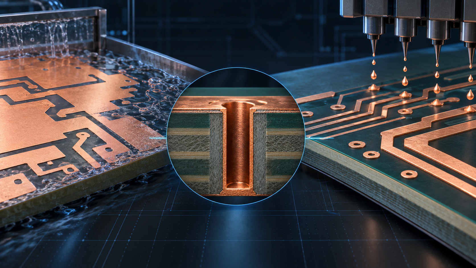
先に答える。P-Flexから発展したSustainaCircuitsは必要箇所へ銅の下地を描く製造方式、DeepViaは深いビアの内壁にめっき用シード層を作る方式、DS-SAPは表面用とビア用のシード形成を分離する方式である。すべてを「配線印刷」と呼ぶと、すでに量産採用された製品と、顧客評価中の工程技術を混同してしまう。
実装基板全体を扱った前稿でElephantechを入口として取り上げた。本稿では検索で観測された「elephantech 銅配線 量産」という問いに対し、同社公式資料で確認できる工程と証拠だけを一段深く整理する。市場規模、歩留まり、顧客数は公表がない限り補わない。
確認時点:2026年9月14日。会社発表は一次情報だが、量産ライン全体の第三者検証ではない。数値は「会社公表値」「本稿の計算」「シナリオ」を明示的に分ける。
| 論点 | 結論 |
|---|
| 同じ技術か | 共通資産は銅ナノ粒子・インク・インクジェット制御だが、対象工程は異なる |
| 量産の証拠 | SustainaCircuits FPCはLogitech製品への量産採用が公表済み |
| 評価段階の技術 | DeepVia HDIとDS-SAPは試験結果や顧客評価を公表しているが、量産歩留まり・出荷数量は未公表 |
| 投資上の確認点 | 技術デモより、装置納入、顧客認定、繰返し受注、材料消費、歩留まりの順で追う |
この区分を保つだけで、「量産している会社だから新工程も量産済み」という誤読を避けられる。
資料を読み比べて最も重要だと感じたのは、銅ナノ粒子そのものより「どこに、何のための銅を置くか」の違いだった。
Elephantechの材料ページによれば、銅ナノ粒子の平均粒径は約15nm、D50は13.4nmである。インクの安定性、焼結性、基材への密着性に加え、primerが液滴の着弾と配線形状を制御する。ここまでは共通技術だが、最終製品までの流れは次の3系統に分かれる。
| 系統 | 銅ナノ粒子を置く場所 | 後工程 | 公式資料で確認できる段階 |
|---|
| SustainaCircuits FPC | 基材表面の回路パターン | 銅めっきで必要厚さまで成長 | 2020年から量産、2025年にLogitechのMX Verticalへ量産採用 |
| DeepVia HDI | HDI基板のビア内壁 | 還元処理で連続膜化し、電解銅めっき | AR 3〜4の試作範囲、2026年8月更新で1,000温度サイクル合格、複数社評価中 |
| DS-SAP | package substrateのビア内、不足するシード部分 | 表面の極薄seedと分離し、pattern plating | 25μm底径ビアの断面例、AI半導体・advanced packaging企業が評価中 |
従来のsubtractive法は、面全体の銅箔から不要部分を除去する。SustainaCircuitsはprimer上に銅ナノインクを印刷し、そこを起点にめっきで導体を成長させる。会社は2025年4月時点で銅使用量を従来比70〜80%削減すると公表し、3〜12μmのFPCに加えて、100μmまでの厚銅FPCを量産中、200μmは開発可能と説明している。
ただし、70〜80%は会社の製品・評価境界に基づく公表値であり、すべての配線密度や層構成へ一律に適用できる係数ではない。LogitechのMX Verticalへの採用は「製品量産」の証拠だが、採用面積、単価、年間数量は公表資料からは分からない。
2025年12月のCu Nano Direct Platingは、desmear後のビア内壁へ銅ナノ粒子を吸着させ、還元処理で連続した銅seedを作り、その後に電解めっきする。公式試験では、上部径0.1mm、絶縁層0.06mm、目標めっき厚20μmの4層HDI test vehicleが、−65℃と125℃を各15分とする700サイクルを通過し、抵抗変化は±10%以内だった。
2026年4月のDeepVia HDIでは、self-wetting inkにより高ARへ範囲を広げた。会社公表の比較は、従来の無電解銅めっきがAR 1.0〜1.2、DeepViaがAR 3〜4である。さらに2026年8月更新の試験は、底径0.1mm、絶縁層0.2mm、目標めっき厚20μm、−55℃と125℃を各15分、1,000サイクル、抵抗変化±5%以内で合格としている。試験条件が違うため、700から1,000への単純な性能向上率は計算しない。
通常のSAPでは、表面とビア内へ同時にseedを形成する。表面seedを厚くすると除去時間と導体損失が増え、微細化には不利になる。一方、薄くしすぎるとビア底の連続性を保ちにくい。DS-SAPは表面に無電解銅またはPVDの極薄seedを作り、ビアだけを銅ナノインクで補完する。
ここで「インクでビアを埋める」と理解するのは誤りである。公式断面例が示すのはABF GL-102上の底径25μmビアにおけるseed補完と、その後の電解めっきの連続性だ。最終導体をインクだけで充填する工程ではない。発表時点は複数企業での評価開始で、量産認定や歩留まりは未開示である。
環境効果の数字を見るとき、私は会社公表値をそのまま横展開せず、まず配線面積だけの幾何モデルを置く。
本稿の計算は、1m²の単層、銅厚18μm、銅密度8,960kg/m³を仮定する。全面銅箔の質量は161.28gである。最終的に銅が残る面積率を30%、50%、70%とすると、subtractive法で除去される銅の理論質量は次のようになる。
| 最終配線の面積率 | 最終配線に残る銅 | 全面銅箔から除去する理論量 | 除去率 |
|---|
| 30% | 48.38g | 112.90g | 70% |
| 50% | 80.64g | 80.64g | 50% |
| 70% | 112.90g | 48.38g | 30% |
計算は次のPythonで再現できる。
COPPER_DENSITY_KG_M3 = 8_960
AREA_M2 = 1.0
THICKNESS_M = 18e-6

full_foil_g = COPPER_DENSITY_KG_M3 * AREA_M2 * THICKNESS_M * 1_000

for coverage in (0.30, 0.50, 0.70):
    final_g = full_foil_g * coverage
    removed_g = full_foil_g - final_g
    print(coverage, round(final_g, 2), round(removed_g, 2))
これは会社の70〜80%削減値を「検証」する計算ではない。additive法にもseed、めっき浴、edge loss、不良、洗浄、再加工があり、subtractive法には銅回収がある。本式が示すのは、配線面積率だけでも理論上の除去量が30〜70%へ動くことだ。したがって、環境・原価比較では層数、panel utilization、完成銅厚、回収率、良品率を揃える必要がある。
ARについても同じ注意が要る。絶縁層300μm、ビア径100μmならARは3.0で、200μmと100μmなら2.0である。DeepViaのAR 3〜4という会社公表レンジは、従来公表レンジ1.0〜1.2の約2.5〜4倍だが、これは幾何学的な到達範囲の比較であり、line throughputやyieldが同じ倍率で改善する意味ではない。
技術の新規性より、証拠がどの段階まで進んだかを分けるほうが投資判断には有用だと考える。
| 証拠段階 | 今回確認できた例 | 次に必要な情報 | まだ言えないこと |
|---|
| 材料・機構 | 約15nm銅粒子、primer、self-wetting | 保存安定性、lot間ばらつき、焼結window | 高歩留まりで量産できる |
| coupon / test vehicle | 25μmビア断面、700または1,000温度サイクル | sample数、failure distribution、追加stress | 製品寿命全体を保証する |
| 顧客評価 | DeepViaとDS-SAPで複数社評価 | qualification完了、装置acceptance | 受注・売上が確定した |
| 製品量産 | Logitech MX VerticalへのFPC採用 | 採用面積、継続期間、他製品への展開 | 新しいvia工程も量産済み |
第一は材料量産である。2025年の資料は銅ナノインクの安定した量産工程に言及するが、それだけで顧客のHDIラインが認定済みとはならない。第二は自社FPC製品の量産で、Logitech採用がここに当たる。第三は顧客工場への装置・材料導入であり、DeepViaやDS-SAPの将来売上を考えるなら、この第三段階の装置acceptanceとrepeat orderが重要になる。
もう一つの落とし穴は、信頼性試験の合格をyieldと呼ぶことだ。温度サイクルの抵抗変化は重要な証拠だが、panel内の全viaの分布、欠陥密度、takt time、maintenance頻度は別指標である。公表がない値を業界平均で埋めると、精密に見えても検証不能になる。
Elephantechは本稿確認時点で上場株式の直接投資対象ではない。したがって個別株の割安・割高は評価しない。採用する見方は、短期はFPC量産採用の継続を確認し、中期は装置・材料モデルが顧客工場でrepeatableになるかを追うこと。却下する見方は、AI向け評価開始だけを根拠に、売上規模や上場企業への利益寄与を逆算することだ。
関連する上場企業や顧客候補への波及を検討する場合でも、契約当事者、売上認識、部材単価が開示されるまで数字を足さない。AI半導体スタートアップのDD観点や、後工程バリューチェーンの確認項目と同じく、「技術が必要」と「投資収益が出る」の間を契約と量産データで埋める必要がある。
現時点では、FPC製品とvia向け装置・材料は異なる速度で進む、という中心仮説が最も無理が少ない。
| シナリオ | 仮定 | 観測する証拠 | 見方を変える条件 |
|---|
| ベースケース | FPC採用は拡大、DeepVia / DS-SAPは評価継続 | 既存採用品の継続、新規test vehicle | 評価時期だけが繰り返し延びる |
| メインシナリオ | 装置とインクを組み合わせた顧客導入が始まる | 装置納入、acceptance、材料repeat order | 顧客工程でthroughputかyieldが成立しない |
| 上振れ | package substrateで量産認定へ進む | qualification完了、量産用途、供給能力 | 単一顧客・単一用途への依存が高い |
| テールリスク | 信頼性、maintenance、原価で導入が遅れる | 仕様変更、納入延期、追加評価 | 独立した複数顧客が同条件で採用する |
次に確認したい数字は5つある。良品panelベースのyield、via径とARごとの欠陥分布、装置takt time、インク消費量と交換頻度、顧客qualificationからrepeat orderまでの期間だ。これらが揃えば、銅ナノ粒子の面白さを、量産能力とunit economicsの議論へ進められる。
結論は限定的だ。SustainaCircuits FPCには製品量産の証拠がある。DeepViaには条件付きのreliability evidenceがあり、DS-SAPには工程断面と顧客評価の証拠がある。ただし後二者には量産歩留まりと出荷数量の証拠がまだない。この線を守ることが、Elephantechを過小評価も過大評価もしない最短ルートだと思う。
次号の記事案
- 案1:DeepViaの量産DDチェックリスト — via径、AR、温度サイクル、panel yieldを同じ条件で比較するテンプレートを作る。
- 案2:ガラスとABFでseed形成はどう変わるか — PVD、無電解銅、銅ナノインクのstep coverageと界面信頼性を一次資料で比べる。
- 案3:PCB装置ビジネスのrepeat revenue — 装置売切り、インク消耗品、保守の収益認識を、開示された契約だけで追跡する。
本記事は情報提供を目的とし、特定銘柄や未上場株式の取得を推奨するものではありません。筆者が記載企業または関連企業の証券を保有する可能性があります。調査・執筆・翻訳に生成AIを利用しています。計算は明示した仮定に基づき、製品性能、量産歩留まり、投資収益を保証しません。詳細は免責事項をご確認ください。
Elephantech Copper Interconnect Technology: Where P-Flex, DeepVia, and DS-SAP Change PCB Manufacturing
Elephantech is often summarized as a company that “prints copper with inkjet.” That description is directionally useful but no longer sufficient. Once the company’s disclosures through 2026 are placed in process order, copper nanoparticles perform different jobs in production FPC surface traces, HDI via walls, and semiconductor package substrates.
The direct answer is this: SustainaCircuits, which evolved from P-Flex, draws a copper foundation only where surface conductors are needed; DeepVia forms a plating seed on the walls of deep vias; and DS-SAP separates the seed requirements of the surface from those of the vias. Calling all three “printed wiring” blurs the line between a product already adopted in mass production and process technologies still undergoing customer evaluation.
The previous substrate overview used Elephantech as one entry point into advanced packaging. This article answers the more specific search intent—where Elephantech changes copper interconnect manufacturing and what “mass production” currently means—using only process details and evidence visible in official material. It does not fill undisclosed market size, yield, customer count, or financial figures with estimates.
Verification date: September 14, 2026. Company releases are primary sources for the company’s claims, not independent audits of complete production lines. Every number below is labeled as a company disclosure, an article calculation, or a scenario.
| Question | Answer |
|---|
| Is it one technology? | Copper nanoparticles, ink formulation, and inkjet control are shared assets, but the target process step differs |
| What has production evidence? | SustainaCircuits FPC has a disclosed mass-production adoption in a Logitech product |
| What remains at evaluation stage? | DeepVia HDI and DS-SAP have test results or customer evaluations, but no disclosed production yield or shipment volume |
| What matters for an investment view? | Track equipment delivery, customer qualification, repeat orders, material consumption, and yield after the technical demo |
Keeping these categories separate prevents a common inference: that because the company manufactures one product at volume, every newer process is already production-qualified.
The most useful distinction in the source material is not the copper nanoparticle itself. It is where copper is placed and what function it serves.
Elephantech’s materials page describes copper nanoparticles with an average size of about 15nm and a D50 of 13.4nm. Ink stability, sinterability, substrate adhesion, and a primer that controls droplet landing and trace shape form a common technology base. The flows to the finished interconnect are nevertheless different.
| Family | Where the nanoparticle copper goes | Subsequent step | Stage supported by official material |
|---|
| SustainaCircuits FPC | Surface circuit pattern on the substrate | Copper plating grows the conductor to target thickness | In production since 2020; disclosed mass-production adoption in Logitech MX Vertical in 2025 |
| DeepVia HDI | Inner wall of an HDI via | Reduction creates a continuous film, followed by electrolytic copper plating | Prototype AR range of 3–4; 1,000 temperature-cycle pass in an August 2026 update; multiple evaluations underway |
| DS-SAP | Insufficient seed regions inside package-substrate vias | Combined with an independently formed ultra-thin surface seed and pattern plating | Cross-section for a 25μm-bottom-diameter via; evaluation by AI semiconductor and advanced-packaging companies |
A subtractive flow begins with copper across the surface and removes the unwanted portion. SustainaCircuits prints copper nanoink on a primer only where a circuit is required, then grows conductor thickness by plating. In April 2025, the company claimed 70–80% less copper use than conventional methods. It described production of FPC conductors up to 100μm thick, development capability up to 200μm, and expansion beyond the existing 3–12μm range.
The 70–80% figure belongs to the company’s stated product and assessment boundary. It is not a universal factor for every trace density or layer stack. The MX Vertical adoption is evidence of product-level mass production, but the release does not disclose adopted area, unit price, or annual volume.
The December 2025 Cu Nano Direct Plating flow adsorbs copper nanoparticles onto desmeared via walls, uses a reduction treatment to create a continuous copper seed, and then applies electrolytic plating. In the disclosed test, a four-layer HDI vehicle with a 0.1mm top via diameter, 0.06mm dielectric, and 20μm target plating passed 700 cycles between −65°C and 125°C, with 15 minutes at each extreme and resistance variation within ±10%.
DeepVia HDI extended the disclosed range in April 2026 through a self-wetting ink for high-aspect-ratio structures. The company compares a conventional electroless-copper range of AR 1.0–1.2 with DeepVia at AR 3–4. Its August 2026 reliability update reports a 0.1mm bottom diameter, 0.2mm dielectric, 20μm target plating, 1,000 cycles between −55°C and 125°C with 15-minute dwells, and resistance variation within ±5%. Because the test vehicles and criteria differ, the move from 700 to 1,000 cycles is not a valid percentage performance improvement.
In a conventional SAP flow, surface and via seeds are formed together. A thicker surface seed increases removal time and conductor loss, which works against fine lines. A seed that is too thin, however, can leave discontinuities at the via bottom. DS-SAP places an ultra-thin electroless-copper or PVD seed on the surface and selectively supplements only the via with copper nanoink.
It would be inaccurate to describe this as filling the via with ink. The official cross-section shows seed supplementation, followed by electroplating, in an ABF GL-102 structure with a 25μm via-bottom diameter. The ink is not the entire final conductor fill. At announcement, multiple AI semiconductor and advanced-packaging companies had begun evaluations; production qualification and yield were not disclosed.
When an environmental claim is expressed as one percentage, I prefer to start with a geometry-only model rather than applying the company figure to unrelated boards.
The article calculation assumes one square meter of a single layer, 18μm copper thickness, and copper density of 8,960kg/m³. Full-area copper mass is 161.28g. If the final conductor covers 30%, 50%, or 70% of the area, the theoretical amount removed by a subtractive flow is as follows.
| Final conductor coverage | Copper left in the traces | Theoretical removal from full foil | Removal ratio |
|---|
| 30% | 48.38g | 112.90g | 70% |
| 50% | 80.64g | 80.64g | 50% |
| 70% | 112.90g | 48.38g | 30% |
The calculation is reproducible with the same Python used in the Japanese section.
COPPER_DENSITY_KG_M3 = 8_960
AREA_M2 = 1.0
THICKNESS_M = 18e-6

full_foil_g = COPPER_DENSITY_KG_M3 * AREA_M2 * THICKNESS_M * 1_000

for coverage in (0.30, 0.50, 0.70):
    final_g = full_foil_g * coverage
    removed_g = full_foil_g - final_g
    print(coverage, round(final_g, 2), round(removed_g, 2))
This does not “validate” the company’s 70–80% reduction claim. Additive processing still has seed material, plating baths, edge losses, defects, washing, and rework; subtractive processing may recover copper. The narrow result is that trace coverage alone moves theoretical removal between 30% and 70%. A useful environmental or cost comparison therefore needs matched layer count, panel utilization, finished copper thickness, recovery rate, and good-unit yield.
Aspect ratio needs the same discipline. A 300μm dielectric divided by a 100μm via diameter gives AR 3.0; 200μm divided by 100μm gives AR 2.0. The company’s DeepVia range of 3–4 is roughly 2.5 to 4 times the disclosed conventional range of 1.0–1.2, but that is a geometric capability comparison. It does not imply the same multiple in line throughput or production yield.
For an investment case, separating the maturity of the evidence is more useful than ranking novelty.
| Evidence stage | Example observed here | Information still needed | What it does not establish |
|---|
| Material and mechanism | About 15nm copper particles, primer, self-wetting behavior | Storage stability, lot variation, sintering window | High-yield production |
| Coupon or test vehicle | 25μm via cross-section; 700- or 1,000-cycle tests | Sample size, failure distribution, additional stresses | Full product lifetime |
| Customer evaluation | Multiple evaluations for DeepVia and DS-SAP | Qualification completion and equipment acceptance | Confirmed orders or revenue |
| Product mass production | FPC adoption in Logitech MX Vertical | Adopted area, duration, expansion to other products | Production status of the new via processes |
The first is material production. The 2025 release says a stable production process exists for the copper nanoink, but that does not mean an HDI line at a customer is qualified. The second is production of Elephantech’s FPC product, for which Logitech is concrete adoption evidence. The third is deployment of equipment and consumable material into customer factories. Equipment acceptance and repeat material orders—not the existence of an FPC factory—will matter most to the future economics of DeepVia or DS-SAP.
A second pitfall is calling a reliability-test pass “yield.” Temperature-cycle resistance is meaningful evidence, but panel-wide via distributions, defect density, takt time, and maintenance frequency are separate variables. Filling those gaps with an industry average would create a precise-looking but unverifiable model.
Elephantech is not a directly investable listed equity as of this review, so this article makes no valuation call. The adopted view is to verify continuity of production FPC adoption in the near term and whether the equipment-plus-material model becomes repeatable at customer sites over the medium term. The rejected view is to infer revenue scale or profit contribution to listed companies solely from the start of AI-related evaluations.
Even when considering read-throughs to listed suppliers or prospective customers, I would not add a financial figure until the contracting party, revenue recognition, and unit economics are disclosed. The same discipline used in the AI semiconductor startup diligence framework and the back-end value-chain checklist applies here: contracts and production data have to bridge “technically needed” and “financially valuable.”
The least demanding central hypothesis is that FPC products and via-oriented equipment/materials will progress at different speeds.
| Scenario | Assumption | Evidence to watch | Condition that changes the view |
|---|
| Base case | FPC adoption expands while DeepVia / DS-SAP remain in evaluation | Continuity of current adoption and new test vehicles | Evaluation dates repeatedly slip without qualification |
| Main scenario | Customer deployment begins with bundled equipment and ink | Equipment delivery, acceptance, repeat material orders | Throughput or yield fails at a customer process |
| Upside | A package-substrate use reaches production qualification | Qualification completion, production application, supply capacity | Dependence remains concentrated in one customer or use case |
| Tail risk | Reliability, maintenance, or cost delays adoption | Specification changes, delivery delays, added evaluations | Multiple independent customers adopt under comparable conditions |
Five measurements would materially improve the analysis: good-panel yield, the defect distribution by via diameter and AR, equipment takt time, ink consumption and replacement frequency, and elapsed time from customer qualification to repeat order. Those data would move the discussion from interesting nanoparticles to production capability and unit economics.
The conclusion is intentionally bounded. SustainaCircuits FPC has product-level production evidence. DeepVia has condition-specific reliability evidence. DS-SAP has process cross-sections and customer-evaluation evidence. The latter two still lack disclosed mass-production yield and shipment volume. Holding that line is the shortest route to avoiding both underestimating and overclaiming Elephantech’s progress.
Next Issue Ideas
- Idea 1: A production-diligence checklist for DeepVia — Compare via diameter, AR, thermal cycling, and panel yield under matched conditions.
- Idea 2: How seed formation changes on glass and ABF — Use primary sources to compare PVD, electroless copper, and copper nanoink on step coverage and interface reliability.
- Idea 3: Repeat revenue in PCB equipment businesses — Track equipment sales, ink consumables, and service revenue using disclosed contracts rather than assumed attach rates.
- Elephantech: Copper nanoparticles, inks, and primer technology
- Elephantech: Thin- and thick-copper SustainaCircuits FPC production, April 9, 2025
- Elephantech: Mass-production adoption in Logitech MX Vertical, April 21, 2025
- Elephantech: Cu Nano Direct Plating and the 700-cycle test, December 23, 2025
- Elephantech: DeepVia HDI AR range and 1,000-cycle test, April 24, 2026, updated August
- Elephantech: DS-SAP process and customer evaluations, June 18, 2026
This article is for informational purposes and is not a recommendation to buy any listed or private security. The author may hold securities issued by companies mentioned here or related companies. Generative AI assisted research, drafting, and translation. Calculations use stated assumptions and do not guarantee product performance, production yield, or investment returns. See the full disclaimer.